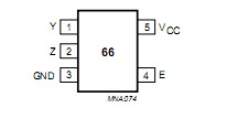
Features: • Wide operating voltage range from 2.0 to 9.0 V
• Very low ON-resistance:
45 Ω (typical) at VCC = 4.5 V
30 Ω (typical) at VCC = 6.0 V
25 Ω (typical) at VCC = 9.0 V.
• High noise immunity
• Low power dissipation
• Very small 5 pins package
• Output capability: non standard.Pinout Specifications
|
SYMBOL |
PARAMETER |
CONDITIONS |
MIN. |
MAX. |
UNIT |
|
VCC |
supply voltage |
|
−0.5 |
+11.0 |
V |
|
IIK |
input diode current |
VI <− 0.5 V or VI > VCC + 0.5 V |
− |
±20 |
mA |
|
ISK |
switch diode current |
VS <− 0.5 V or VS > VCC + 0.5 V |
− |
±20 |
mA |
|
IS |
switch source or sink current |
−0.5 V < VS < VCC + 0.5 V |
− |
±25 |
mA |
|
ICC |
VCC or GND current |
|
− |
±50 |
mA |
|
Tstg |
storage temperature |
|
−65 |
+150 |
|
|
PD |
power dissipation per package |
or temperature range from −40 to + 125 ; note 2 |
− |
200 |
mW |
|
PS |
power dissipation per switch |
|
− |
100 |
mW |
Notes
1. To avoid drawing V
CC current out of pin Z, when switch current flows in pin
Y, the voltage drop across the bidirectional switch must not exceed 0.4 V.
If the switch current flows into pin Z, no V
CC current will flow out of terminal
Y. In this case there is no limit for the voltage drop across the switch, but
the voltage at pins Y and Z may not exceed V
CC or GND.
2. Above 55
the value of P
D derates linearly with 2.5 mW/K.
DescriptionThe 74HC1G66 is a high-speed Si-gate CMOS device.
The 74HC1G66 provides an analog switch. The switch has two input/output pins (Y and Z) and an active HIGH enable input pin (E).When pin E is LOW, the analog switch is turned off.
The non standard output currents pf the 74HC1G66 are equal compared to the 74HC/HCT4066.

 74HC1G66 Data Sheet


