74HCT670

Features: · Simultaneous and independent read and write operations· Expandable to almost any word size and bit length· Output capability: bus driver· ICC category: MSIPinoutDescriptionThe 74HCT670 ishigh-speed Si-gate CMOS devices and are pin compatible with low power Schottky TTL (LSTTL). They ar...

product image

74HCT670 Picture
SeekIC No. : 004250944 Detail

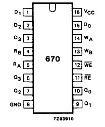
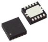
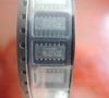
74HCT670: Features: · Simultaneous and independent read and write operations· Expandable to almost any word size and bit length· Output capability: bus driver· ICC category: MSIPinoutDescriptionThe 74HCT670 i...

floor Price/Ceiling Price

Part Number:
74HCT670
Supply Ability:
5000

Price Break

  • Qty
  • 1~5000
  • Unit Price
  • Negotiable
  • Processing time
  • 15 Days
Total Cost: $ 0.00

SeekIC Buyer Protection PLUS - newly updated for 2013!

  • Escrow Protection.
  • Guaranteed refunds.
  • Secure payments.
  • Learn more >>

Month Sales

268 Transactions

Rating

evaluate  (4.8 stars)

Upload time: 2024/4/29

Payment Methods

All payment methods are secure and covered by SeekIC Buyer Protection PLUS.

Notice: When you place an order, your payment is made to SeekIC and not to your seller. SeekIC only pays the seller after confirming you have received your order. We will also never share your payment details with your seller.
Product Details

Description


Features:

· Simultaneous and independent read and write operations
· Expandable to almost any word size and bit length
· Output capability: bus driver
· ICC category: MSI


Pinout

  Connection Diagram


Description

The 74HCT670 is high-speed Si-gate CMOS devices and are pin compatible with low power Schottky TTL (LSTTL). They are specified in compliance with JEDEC standard no. 7A.

The 74HCT670 is 16-bit 3-state register files organized as 4 words of 4 bits each. Separated read and write address inputs (RA, RB and WA, WB) and enable inputs (RE and WE) are available, permitting simultaneous writing into one word location and reading from another location. The 4-bit word to be stored is presented to four data inputs (D0 to D3). The WA and WB inputs determinethe location of the stored word. When theWE input is LOW, the data is entered into the addressed location. The addressed location remains transparent to the data while theWE input is LOW. Data supplied at the inputs will be read out in true (non-inverting) form from the 3-state outputs (Q0 to Q3). Dn and Wn inputs are inhibited when WE is HIGH.

Direct acquisition of data stored in any of the four registers of the 74HCT670 is made possible by individual read address inputs (RA and RB). The addressed word appears at the four outputs when theRE is LOW. Data outputs are in the high impedance OFF-state when RE is HIGH. This permits outputs to be tied together to increase the word capacity to very large numbers.

Design of the read enable signals for the stacked devices must ensure that there is no overlap in the LOW levels which would cause more than one output to be active at the same time. Parallel expansion to generate n-bit words is accomplished by driving the enable and address inputs of each device in parallel.

The 74HCT670 is designed as high-speed si-gate CMOS devices and are pin compatible with low power schottky TTL (LSTTL). It is specified in compliance with JEDEC standard no. 7A. It is 16-bit 3-state register files organized as 4 words of 4 bits each. Separated read and write address inputs (RA, RB and WA, WB) and enable inputs (RE and WE) are available, permitting simultaneous writing into one word location and reading from another location. Design of the read enable signals for the stacked devices must ensure that there is no overlap in the low levels which would cause more than one output to be active at the same time. Parallel expansion to generate n-bit words is accomplished by driving the enable and address inputs of each device in parallel.

The four features of the 74HCT670. The first one is simultaneous and independent read and write operations. The second one is expandable to almost any word size and bit length. The third one is its output capability is bus driver. The fourth one is its ICC category is MSI. That are all the main features.

Some important AC characteristics and specifications of the 74HCT670 have been concluded into several points as follow.For Tamb=25°C the first one is about its propagation delay RA, RB to Qn which would be typ 58ns and max 195ns at Vcc=2.0V and would be typ 21ns and max 39ns at Vcc=4.5V and would be typ 17ns and max 33ns at Vcc=6.0V. The second one is about its propagation delay Dn to Qn which would be typ 74ns and max 250ns at Vcc=2.0V and typ 27ns and max 50ns at Vcc=4.5V and would be typ 22ns and max 43ns at Vcc=6.0V. The third one is about its 3-state output enable time RE to Qn which would be typ 39ns and max 150ns at Vcc=2.0V and typ 14ns and max 30ns at Vcc=4.5V and would be typ 11ns and max 26ns at Vcc=6.0V. The fourth one is about its output transition time which would be typ 14ns and max 60ns at Vcc=2.0V and typ 5ns and max 12ns at Vcc=4.5V and would be typ 4ns and max 10ns at Vcc=6.0V. And so on. For more information about the 74HCT670 please contact us for details.


Customers Who Bought This Item Also Bought

Margin,quality,low-cost products with low minimum orders. Secure your online payments with SeekIC Buyer Protection.
Motors, Solenoids, Driver Boards/Modules
Boxes, Enclosures, Racks
Circuit Protection
Audio Products
Optoelectronics
View more