74LS166

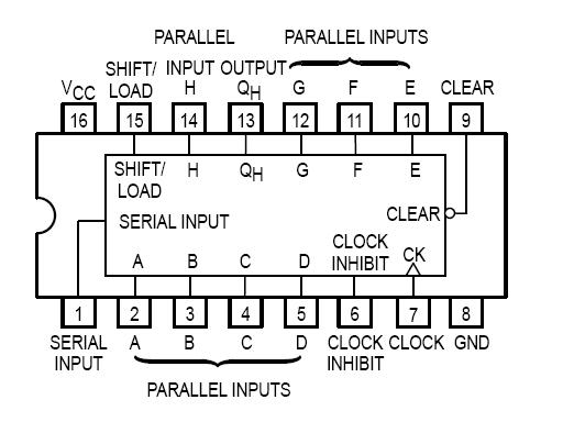
Features: • Synchronous Load• Direct Overriding Clear• Parallel to Serial ConversionPinoutDescriptionThe 74LS166 is an 8-Bit Shift Register. Designed with all inputs buffered, the drive requirements are lowered to one 54/74LS standard load. By utilizing input clamping diodes, swi...

product image

74LS166 Picture
SeekIC No. : 004251087 Detail

74LS166: Features: • Synchronous Load• Direct Overriding Clear• Parallel to Serial ConversionPinoutDescriptionThe 74LS166 is an 8-Bit Shift Register. Designed with all inputs buffered, the ...

floor Price/Ceiling Price

Part Number:
74LS166
Supply Ability:
5000

Price Break

  • Qty
  • 1~5000
  • Unit Price
  • Negotiable
  • Processing time
  • 15 Days
Total Cost: $ 0.00

SeekIC Buyer Protection PLUS - newly updated for 2013!

  • Escrow Protection.
  • Guaranteed refunds.
  • Secure payments.
  • Learn more >>

Month Sales

268 Transactions

Rating

evaluate  (4.8 stars)

Upload time: 2024/4/25

Payment Methods

All payment methods are secure and covered by SeekIC Buyer Protection PLUS.

Notice: When you place an order, your payment is made to SeekIC and not to your seller. SeekIC only pays the seller after confirming you have received your order. We will also never share your payment details with your seller.
Product Details

Description


Features:

• Synchronous Load
• Direct Overriding Clear
• Parallel to Serial Conversion


Pinout

  Connection Diagram


Description

The 74LS166 is an 8-Bit Shift Register. Designed with all inputs buffered, the drive requirements are lowered to one 54/74LS standard load. By utilizing input clamping diodes, switching transients are minimized and system design simplified.

The 74LS166 is a parallel-in or serial-in, serial-out shift register and has a complexity of 77 equivalent gates with gated clock inputs and an overriding clear input. The shift/load input establishes the parallel-in or serial-in mode. When high, this input enables the serial data input and couples the eight flip-flops for serial shifting with each clock pulse. Synchronous loading occurs on the next clock pulse when this is low and the parallel data inputs are enabled. Serial data flow of the 74LS166 is inhibited during parallel loading. Clocking is done on the low-to-high level edge of the clock pulse via a two input positive NOR gate, which permits one input to be used as a clock enable or clock inhibit function. Clocking is inhibited when either of the clock inputs are held high, holding either input low enables the other clock input. This will allow the system clock to be free running and the register stopped on command with the other clock input. A change from low-to-high on the clock inhibit input should only be done when the clock input is high. A buffered direct clear input overrides all other inputs, including the clock, and sets all flip-flops to zero.


Customers Who Bought This Item Also Bought

Margin,quality,low-cost products with low minimum orders. Secure your online payments with SeekIC Buyer Protection.
Crystals and Oscillators
Programmers, Development Systems
Prototyping Products
DE1
Resistors
Batteries, Chargers, Holders
View more