Low Level Output Current
:
Maximum Operating Temperature
: + 125 C
Minimum Operating Temperature
: - 40 C
Polarity
: Non-Inverting
Number of Output Lines
: 8
Number of Circuits
: 1
Packaging
: Tube
High Level Output Current
: - 6 mA
Supply Voltage - Max
: 3.6 V
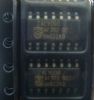
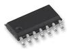
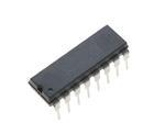
Package / Case
: PDIP-16
Logic Type
: TTL
Logic Family
: LV
Propagation Delay Time
: 17 ns at 3.3 V
Supply Voltage - Min
: 1 V
DescriptionThe 74LV259N belongs to 74LV259 family which also incorporate an active LOW common reset (MR) for resetting all latches, as well as an active LOW enable input (LE) and is a low-voltage CMOS device and is pin and function compatible with 74HC/HCT259. The 74LV259 has four modes of operation as shown in the mode select table. In the addressable latch mode, data on the data line (D) is written into the addressed latch. The addressed latch of the 74LV259N will follow the data input with all non-addressed latches remaining in their previous states. In the memory mode, all latches remain in their previous states and are unaffected by the data or address inputs. The 74LV259 is a high-speed 8-bit addressable latch designed for general purpose storage applications in digital systems. The 74LV259 is a multifunction device capable of storing single-line data in eight addressable latches, and also 3-to-8 decoder and demultiplexer, with active HIGH outputs (Q0 to Q7), functions are available.
The features of 74LV259N can be summarized as (1)optimized for low voltage applications: 1.0 to 3.6 V; (2)accepts TTL input levels between VCC = 2.7 V and VCC = 3.6 V; (3)typical VOLP (output ground bounce) < 0.8 V at VCC = 3.3 V, Tamb = 25°C; (4)typical VOHV (output VOH undershoot) > 2 V at VCC = 3.3 V, Tamb = 25°C; (5)combines demultiplexer and 8-bit latch; (6)serial-to-parallel capability; (7)output from each storage bit available; (8)random (addressable) data entry; (9)easily expandable; (10)common reset input; (11)useful as a 3-to-8 active HIGH decoder; (12)output capability of the 74LV259N: standard; (13)ICC category: MS.
The absolute maximum ratings of 74LV259N are (1)VCC DC supply voltage: -0.5 to +4.6 V; (2)±IIK DC input diode current(VI < -0.5 or VI > VCC + 0.5V): 20 mA; (3)±IOK DC output diode current(VO < -0.5 or VO > VCC + 0.5V): 50 mA; (4)±IO DC output source or sink current- standard outputs(-0.5V < VO < VCC + 0.5V): 25 mA; (5)±IGND, ±ICC DC VCC or GND current for types with-standard outputs: 50 mA; (6)Tstg storage temperature range of the 74LV259N: -65 to +150 °C; (7)Ptot power dissipation per package for temperature range: -40 to +125°C,plastic DIL above +70°C derate linearly with 12mW/K/plastic mini-pack (SO) above +70°C derate linearly with 8 mW/K/plastic shrink mini-pack (SSOP and TSSOP)above +60°C derate linearly with 5.5 mW/K: 750/500/400mW.(1. Stresses beyond those listed may cause permanent damage to the device. These are stress ratings only and functional operation of the device at these or any other conditions beyond those indicated under "recommended operating conditions" is not implied. Exposure to absolute maximum rated conditions for extended periods may affect device reliability. 2. The input and output voltage ratings of the 74LV259N may be exceeded if the input and output current ratings are observed.).
 74LV259N Data Sheet