Logic Family
:
Number of Bits
:
Counting Method
:
Counting Sequence
:
Operating Supply Voltage
:
Operating Temperature Range
:
Counter Type
: Binary Counters
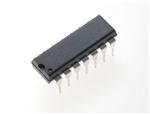
Packaging
: Tube
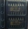
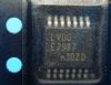
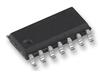
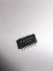
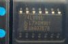
Package / Case
: SOT-27
DescriptionThe 74LV393N belongs to 74LV393 family which is a dual 4-bit binary ripple counter with separate clocks (1CP, 2CP) and master reset (1MR, 2MR) inputs to each counter. The operation of each half of the "393" is the same as the "93" except no external clock connections are required. The counters are triggered by a HIGH-to-LOW transition of the clock inputs. The counter outputs of the 74LV393N are internally connected to provide clock inputs to succeeding stages. The outputs of the ripple counter do not change synchronously and should not be used for high-speed address decoding. The master resets are active-HIGH asynchronous inputs to each 4-bit counter identified by the "1" and "2" in the pin description. A HIGH level on the nMR input overrides the clock and sets the outputs LOW. The 74LV393 is a low±voltage Si-gate CMOS device and is pin and function compatible with 74HC/HCT393.
The features of 74LV393N can be summarized as (1)optimized for low voltage applications: 1.0 to 3.6V; (2)accepts TTL input levels between VCC = 2.7V and VCC = 3.6V; (3)typical VOLP (output ground bounce)< 0.8V @ VCC = 3.3V, Tamb = 25°C; (4)typical VOHV (output VOH undershoot) <2V @ VCC = 3.3V, Tamb = 25°C; (5)two 4-bit binary counters with individual clocks; (6)divide-by any binary module up to 28 in one package; (7)two master resets to clear each 4-bit counter individually; (8)output capability: standard; (9)ICC category: MSI.
The absolute maximum ratings of 74LV393N are (1)VCC DC supply voltage: -0.5 to +4.6 V; (2)±IIK DC input diode current(VI < -0.5 or VI > VCC + 0.5V): 20mA; (3)±IOK DC output diode current(VO < -0.5 or VO > VCC + 0.5V): 50mA; (4)±IO DC output source or sink current -bus driver outputs(-0.5V < VO < VCC + 0.5V): 25mA; (5)±IGND, ±ICC DC VCC or GND current for types with bus driver outputs: 50mA; (6)Tstg storage temperature range: -65 to +150 °C; (7)power dissipation per package for temperature range of the 74LV393N: -40 to +125°C-plastic DIL(above +70°C derate linearly with 12mW/K)/-plastic mini-pack (SO)(above +70°C derate linearly with 8 mW/K)/-plastic shrink mini-pack (SSOP and TSSOP)(above +60°C derate linearly with 5.5 mW/K): 750/500/400mW.(1. Stresses beyond those listed may cause permanent damage to the device. These are stress ratings only and functional operation of the device at these or any other conditions beyond those indicated under arecommended operating conditionso is not implied. Exposure to absolute-maximum-rated conditions for extended periods may affect device reliability. 2. The input and output voltage ratings of the 74LV393N may be exceeded if the input and output current ratings are observed.)
 74LV393N Data Sheet