74LVC06AD

Buffers & Line Drivers HEX INVERTER/BUF DRV

product image

74LVC06AD Picture
SeekIC No. : 00411625 Detail

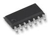
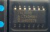
74LVC06AD: Buffers & Line Drivers HEX INVERTER/BUF DRV

floor Price/Ceiling Price

Part Number:
74LVC06AD
Mfg:
NXP Semiconductors
Supply Ability:
5000

Price Break

  • Qty
  • 1~5000
  • Unit Price
  • Negotiable
  • Processing time
  • 15 Days
Total Cost: $ 0.00

SeekIC Buyer Protection PLUS - newly updated for 2013!

  • Escrow Protection.
  • Guaranteed refunds.
  • Secure payments.
  • Learn more >>

Month Sales

268 Transactions

Rating

evaluate  (4.8 stars)

Upload time: 2024/5/4

Payment Methods

All payment methods are secure and covered by SeekIC Buyer Protection PLUS.

Notice: When you place an order, your payment is made to SeekIC and not to your seller. SeekIC only pays the seller after confirming you have received your order. We will also never share your payment details with your seller.
Product Details

Quick Details

Number of Input Lines : 6 Number of Output Lines : 6
Polarity : Inverting Supply Voltage - Max : 5.5 V
Supply Voltage - Min : 1.65 V Maximum Operating Temperature : + 125 C
Mounting Style : SMD/SMT Package / Case : SOT-108-14
Packaging : Tube    

Description

Number of Input Lines : 6
Number of Output Lines : 6
Mounting Style : SMD/SMT
Maximum Operating Temperature : + 125 C
Supply Voltage - Max : 5.5 V
Supply Voltage - Min : 1.65 V
Polarity : Inverting
Packaging : Tube
Package / Case : SOT-108-14


Description

The 74LVC06AD is designed as a high performance low power, low voltage, si-gate CMOS device, superior to most advanced CMOS compatible TTL families. Inputs can be driven from either 3.3V or 5V devices. This feature allows the use of these devices as translators in mixed 3.3V to 5V environment.

The six features of the 74LVC06AD. (1)5V tolerant inputs and outputs (open drain) for interfacing with 5V logic. (2)Wide supply voltage range from 1.65V to 5.5V. (3)CMOS low power consumption. (4)Direct interface with TTL levels. (5)Inputs accept voltages up to 5V. (6)Complies with JEDEC standard no.8-1A. Those are all the main features.

Some absolute maximum ratings of the 74LVC06AD have been concluded into several points as follow. (1)Its DC supply voltage would be from -0.5V to 6.5V. (2)Its DC input diode current would be max -50mA. (3)Its DC input voltage range would be from -0.5V to 6.5V. (4)Its DC output clamping diode current would be max -50mA. (5)Its DC output voltage would be from -0.5V to Vcc+0.5V for active mode and would be from -0.5V to 6.5V for high impedance mode. (6)Its DC output sink current would be max 50mA. (7)Its DC Vcc or GND current would be max +/-100mA. (8)Its storage temperature range of the 74LVC06AD would be from -65°C to 150°C. (9)Its power dissipation would be 500mW. It should be noted that stresses above those listed in absolute maximum ratings may cause permanent damage to device.

Also some electrical characteristics of the 74LVC06AD are concluded as follow. (1)Its high level input voltage would be min Vcc at Vcc=1.65V to 1.95V and would be min 1.7V at 2.3V to 2.7V and would be min 2.0V at 2.7V to 3.6V. (2)Its low level input voltage would be max GND at Vcc=1.65V to 1.95V and would be max 0.7V at Vcc=2.3V to 2.7V and would be max 0.8V at 2.7V to 3.6V. And so on. If you have any question or suggestion or want to know more information about the 74LVC06AD please contact us for details. Thank you!


Customers Who Bought This Item Also Bought

Margin,quality,low-cost products with low minimum orders. Secure your online payments with SeekIC Buyer Protection.
Optical Inspection Equipment
Cables, Wires
Audio Products
Potentiometers, Variable Resistors
Discrete Semiconductor Products
Cable Assemblies
View more