Output Type
:
Low Level Output Current
:
Supply Voltage - Max
: 3.6 V
Mounting Style
: SMD/SMT
Packaging
: Reel
Number of Circuits
: 2
Polarity
: Non-Inverting
Input Type
: Single-Ended
Maximum Operating Temperature
: + 85 C
Logic Type
: D-Type (3-State) Flip-Flop
High Level Output Current
: - 12 mA
Logic Family
: LVT
Propagation Delay Time
: 3.4 ns
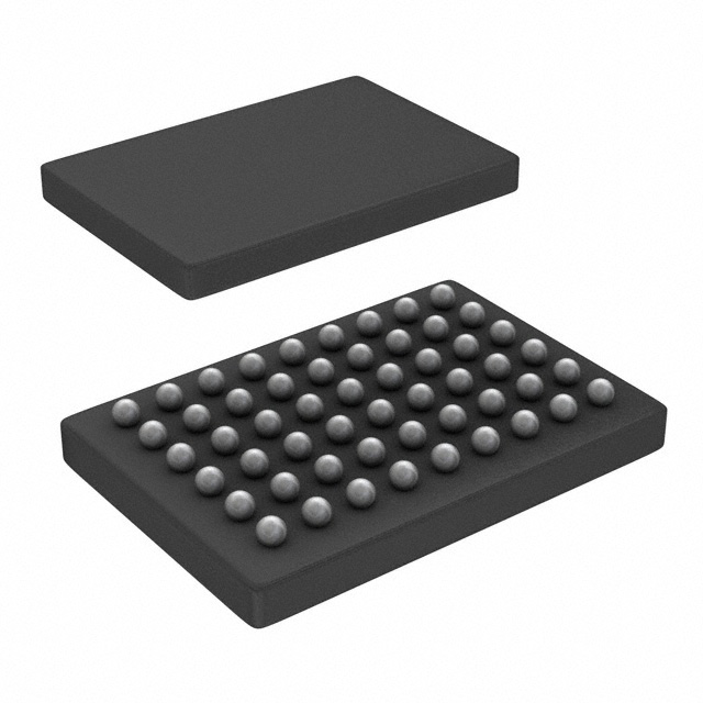
Package / Case
: BGA MICROSTAR JUNIOR-54
Features: ` Members of the Texas Instruments Widebus™ Family
` Output Ports Have Equivalent 22-W Series
Resistors, So No External Resistors Are Required
` Support Mixed-Mode Signal Operation (5-V
Input and Output Voltages With 3.3-V VCC )
` Support Unregulated Battery Operation Down to 2.7 V
` Typical VOLP (Output Ground Bounce) <0.8 V
at VCC = 3.3 V, TA = 25°C
` Ioff and Power-Up 3-State Support Hot Insertion
` Bus Hold on Data Inputs Eliminates the Need
for External Pullup/Pulldown Resistors
` Distributed VCC and GND Pins Minimize
High-Speed Switching Noise
` Flow-Through Architecture Optimizes PCB Layout
` Latch-Up Performance Exceeds 500 mA Per JESD 17
` ESD Protection Exceeds JESD 22
2000-V Human-Body Model (A114-A)
200-V Machine Model (A115-A)Pinout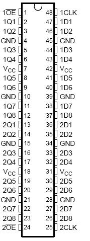 Specifications
| |
MIN |
MAX |
UNIT |
| VCC Supply voltage range |
0.5 |
4.6 |
V |
| VI Input voltage range(2) |
0.5 |
7 |
V |
| VO Voltage range applied to any output in the high-impedance or power-off state(2) |
0.5 |
7 |
V |
| VO Voltage range applied to any output in the high state(2) |
0.5 |
+0.5 |
V |
| IO Current into any output in the low state |
|
30 |
mA |
| IO Current into any output in the high state(3) |
|
30 |
mA |
| IIK Input clamp current |
VI < 0 |
|
-50 |
mA |
| IOK Output clamp current |
VO < 0 |
|
-50 |
mA |
| qJA Package thermal impedance(4) |
DGG package |
|
70 |
°C/W |
| DL package |
|
63 |
| GQL/ZQL package |
|
42 |
| GRD/ZRD package |
|
36 |
| Tstg Storage temperature rang |
-65 |
150 |
°C |
DescriptionThe 74LVTH162374GRDR devices are 16-bit edge-triggered D-type flip-flops with 3-state outputs designed for low-voltage (3.3-V) VCC operation, but with the capability to provide a TTL interface to a 5-V system environment. They are particularly suitable for implementing buffer registers, I/O ports, bidirectional bus drivers, and working registers.
The 74LVTH162374GRDR can be used as two 8-bit flip-flops or one 16-bit flip-flop. On the positive transition of the clock (CLK), the Q outputs of the flip-flop take on the logic levels set up at the D inputs.
A buffered output-enable (OE) input can be used to place the eight outputs in either a normal logic state (high or low logic levels) or a high-impedance state. In the high-impedance state, the outputs neither load nor drive the bus lines significantly. The high-impedance state and the increased drive provide the capability to drive bus lines without need for interface or pullup components.
OE does not affect internal operations of the flip-flop. Old data can be retained or new data can be entered while the outputs are in the high-impedance state.
The outputs, which are designed to source or sink up to 12 mA, include equivalent 22-W series resistors to reduce overshoot and undershoot.
Active bus-hold circuitry holds unused or undriven inputs at a valid logic state. Use of pullup or pulldown resistors with the bus-hold circuitry is not recommended.
When VCC is between 0 and 1.5 V, the devices are in the high-impedance state during power up or power down. However, to ensure the high-impedance state above 1.5 V, OE should be tied to VCC through a pullup resistor; the minimum value of the resistor is determined by the current-sinking capability of the driver.
The 74LVTH162374GRDR are fully specified for hot-insertion applications using Ioff and power-up 3-state. The Ioff circuitry disables the outputs, preventing damaging current backflow through the devices when they are powered down. The power-up 3-state circuitry places the outputs in the high-impedance state during power up and power down, which prevents driver conflict.
Parameters: | Technical/Catalog Information | 74LVTH162374GRDR |
| Vendor | Texas Instruments (VA) |
| Category | Integrated Circuits (ICs) |
| Mounting Type | Surface Mount |
| Package / Case | 54-BGA MICROSTAR JUNIOR |
| Function | Standard |
| Number of Bits per Element | 8 |
| Number of Elements | 2 - Dual |
| Current - Output High, Low | 12mA, 12mA |
| Output Type | Tri-State Non Inverted |
| Trigger Type | Positive Edge |
| Type | D-Type Bus |
| Packaging | Digi-Reel? |
| Operating Temperature | -40°C ~ 85°C |
| Delay Time - Propagation | 3.4ns |
| Frequency - Clock | 160MHz |
| Voltage - Supply | 2.7 V ~ 3.6 V |
| Drawing Number | 296; 4204759; GRD; 54 |
| Lead Free Status | Contains Lead |
| RoHS Status | RoHS Non-Compliant |
| Other Names | 74LVTH162374GRDR
74LVTH162374GRDR
296 16879 6 ND
296168796ND
296-16879-6
|
 74LVTH162374GRDR Data Sheet