Features: · Input and output interface capability to systems at 5V VCC
· Bushold data inputs eliminate the need for external pull-up resistors to hold unused inputs (74LVTH16952)
· Live insertion/extraction permitted
· Power Up/Down high impedance provides glitch-free bus loading
· Outputs source/sink −32 mA/+64 mA
· Functionally compatible with the 74 series 16952
· Latch-up conforms to JEDEC JED78
· ESD performance: Human-body model > 2000V Machine model > 200V Charged-device model > 1000VPinout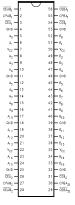 Specifications
| Symbol |
Parameter |
Value |
Conditions |
Units |
| VCC |
Supply Voltage |
−0.5 to +4.6 |
|
V |
| VI |
DC Input Voltage |
−0.5 to +7.0 |
|
V |
| VO |
DC Output Voltage |
−0.5 to +7.0 |
Output in 3-STATE |
V |
| −0.5 to +7.0 |
Output in HIGH or LOW State (Note 3) |
V |
| IIK |
DC Input Diode Current |
−50 |
VI < GND |
mA |
| IOK |
DC Output Diode Current |
−50 |
VO < GND |
mA |
| IO |
DC Output Current |
64 |
VO > VCC Output at HIGH State |
mA |
| 128 |
VO > VCC Output at LOW State |
| ICC |
DC Supply Current per Supply Pin |
±64 |
|
mA |
| IGND |
DC Ground Current per Ground Pin |
±128 |
|
mA |
| TSTG |
Storage Temperature |
−65 to +150 |
|
|
DescriptionThe 74LVTH16952 are 16-bit registered transceivers. Two 8-bit back to back registers store data flowing in both directions between two bidirectional buses.
Separate clock, clock enable, and output enable signals are provided for each register.
The 74LVTH16952 data inputs include bushold, eliminating the need for external pull-up resistors to hold unused inputs.
The registered transceiver is designed for low-voltage (3.3V) VCC applications, but with the capability to provide a TTL interface to a 5V environment.
The 74LVTH16952 are fabricated with an advanced BiCMOS technology to achieve high speed operation similar to 5V ABT while maintaining low power dissipation.
The 74LVTH16952 is 16-bit registered transceivers. Two 8-bit back to back registers store data flowing in both directions between two bidirectional buses. Separate clock, clock enable, and output enable signals are provided for each register. The feature of 74LVTH16952 are as follows: (1)Input and output interface capability to systems at 5V VCC; (2)Bushold data inputs eliminate the need for external pull-up resistors to hold unused inputs (74LVTH16952); (3)Live insertion/extraction permitted; (4)Power Up/Down high impedance provides glitch-free bus loading; (5)Outputs source/sink .32 mA/+64 mA; (6)Functionally compatible with the 74 series 16952; (7)Latch-up conforms to JEDEC JED78; (8)ESD performance: Human-body model > 2000V, Machine model > 200V, Charged-device model > 1000V.
The absolute maximum ratings of the 74LVTH16952 are: (1)Input Clamp Diode Voltage: -1.2 V max at II = -18 mA; (2)Input HIGH Voltage: 2.0V min at VO 0.1V or VO VCC-0.1V; (3)Output HIGH Voltage: VCC-0.2 V min at IOH = -100 A; (4)Output LOW Voltage: 0.2 V max at IOL = 100 A; (5)Bushold Input Minimum Drive: 75 A min at VI = 0.8V; (6)Bushold Input Over-Drive: 500 A min; (7)Input Current: 10 A max at VI = 5.5V; (8)Power Off Leakage Current: ±100 A max at 0V VI or VO 5.5V; (9)Power Up/Down 3-STATE Output Current: ±100 A at VO = 0.5V to 3.0V, VI = GND or VCC; (10)3-STATE Output Leakage Current: -5 A at VO = 3.0V.
The following is about the electrical characteristics of 74LVTH16952: (1)High Level Input Voltage: 2.1V min and 1.5V typical at VO = 0.1 V or VCC-0.1V; (2)low Level Input Voltage: 1.5V typical and 0.9V max at VO = 0.1 V or VCC-0.1V; (3)High Level Output Voltage: 2.9V min and 2.99V typical at IO=-50 A; (4)low Level Output Voltage: 0.002V typical and 0.1V max at IO=-50 A; (5)Input Leakage Current: ±0.1A max at VI = VCC or GND; (6)Quiescent Supply Current: 8A max at VI = VCC or GND; (7)Dynamic Output Current: 75mA max at VOLD = 1.65 V max.

 74LVTH16952 Data Sheet