Number of Channels per Chip
: 8
Output Type
: 3-State
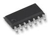
Package / Case
: SOIC-24
Packaging
: Tube
Logic Type
: CMOS
Maximum Operating Temperature
: + 85 C
High Level Output Current
: - 24 mA
Low Level Output Current
: 24 mA
Input Level
: CMOS
Output Level
: CMOS
Propagation Delay Time
: 8 ns
Supply Voltage - Max
: 3.6 V, 5.5 V
Logic Family
: 74LVX
Supply Voltage - Min
: 2.7 V, 4.5 V
DescriptionThe 74LVX3245WM belongs to LVX3245 family which is a dual-supply, 8-bit translating transceiver that is designed to interface between a 3V bus and a 5V bus in a mixed 3V/5V supply environment. The Transmit/ Receive (T/R) input determines the direction of data flow. Transmit (active-HIGH) enables data from A Ports to B Ports; Receive (active-LOW) enables data from B Ports to A Ports. The Output Enable input, when HIGH, disables both A and B Ports by placing them in a high impedance condition. The A Port interfaces with the 3V bus; the B Port interfaces with the 5V bus. The LVX3245 is suitable for mixed voltage applications such as notebook computers using 3.3V CPU and 5V peripheral components.
The features of 74LVX3245WM can be summarized as (1)bidirectional interface between 3V and 5V buses; (2)inputs compatible with TTL level; (3)3V data flow at A Port and 5V data flow at B Port; (4)outputs source/sink 24 mA; (5)guaranteed simultaneous switching noise level and dynamic threshold performance; (6)implements proprietary EMI reduction circuitry; (7)functionally compatible with the 74 series 245.
The absolute maximum ratings of 74LVX3245WM are (1)supply voltage (VCCA, VCCB): 0.5V to +7.0V; (2)DC input voltage (VI) @ OE, T/R: 0.5V to VCCA + 0.5V; (3)DC input/output voltage (VI/O) @ An/@ Bn: -0.5V to VCCA + 0.5V/-0.5V to VCCB + 0.5V; (4)DC input diode current (IIN) @ OE, T/R: ±20mA; (5)DC output diode current (IOK): ±50mA; (6)DC output source or sink current (IO): ±50mA; (7)DC VCC or Ground Current per Output Pin (ICC or IGND)/and Max Current @ ICCA/@ ICCB: ±50/±100/±200mA; (8)The storage temperature range of the 74LVX3245WM (TSTG): -65°C to +150°C; (9)DC latch-up source or sink current: ±300mA. (Absolute Maximum Ratings are those values beyond which the safety of the device cannot be guaranteed. The device should not be operated at these limits. The parametric values defined in the Electrical Characteristics tables are not guaranteed at the absolute maximum ratings. )
 74LVX3245WM Data Sheet