Features: • 5V and 3.3V Families fully compatible with JEDEC
specifications
• Up to 2000 Gate Array Gates (6000 PLD equivalent gates)
• Replaces up to 50 TTL Packages
• Replaces up to twenty 20-Pin PAL® Packages
• Design Library with over 250 Macro Functions
• Gate Array Architecture Allows Completely Automatic
Place and Route
• Up to 547 Programmable Logic Modules
• Up to 273 Flip-Flops
• Data Rates to 75 MHz
• Two In-Circuit Diagnostic Probe Pins Support Speed
Analysis to 25 MHz
• Built-In High Speed Clock Distribution Network
• I/O Drive to 10 mA (5 V), 6 mA (3.3 V)
• Nonvolatile, User Programmable
• Fabricated in 1.0 micron CMOS technologyPinout SpecificationsVCC DC Supply Voltage2 ........0.5 to +7.0 Volts
VI Input Voltage............. 0.5 to VCC +0.5 Volts
VO Output Voltage .........0.5 to VCC +0.5 Volts
IIO I/O Sink/Source Current3.................±20 mA
TSTG Storage Temperature .........65 to +150DescriptionThe A1010B is designed as one member of the ACT 1 series of field programmable gate arrays (FPGAs) which offers a variety of package, speed, and application combinations. A1010B is implemented in silicon gate, 1-micron two-level metal CMOS, and they employ actel's PLICE antifuse technology. The unique architecture of A1010B offers gate array flexibility, high performance, and instant turnaround through user programming. Device utilization is typically 95 to 100 percent of available logic modules.
A1010B has many features. (1)5V and 3.3V families fully compatible with JEDEC specifications. (2)Up to 2000 gate array gates (6000 PLD equivalent gates). (3)Replaces up to 50 TTL packages. (4)Replaces up to twenty 20-pin PAL packages. (5)Design library with over 250 macro functions. (6)Gate array architecture allows completely automatic place and route. (7)Up to 547 programmable logic modules. (8)Up to 273 flip-flops. (9)Data rates to 75MHz. (10)Two in-circuit diagnostic probe pins support speed analysis to 25MHz. And so on.
Some absolute maximum ratings of A1010B have been concluded into several points as follow. (1)Its DC supply voltage would be from -0.5V to 7.0V. (2)Its input voltage would be from -0.5V to Vcc+0.5V. (3)Its output voltage would be from -0.5V to Vcc+0.5V. (4)Its I/O sink/source current would be +/-20mA. (5)Its storage temperature range would be from -65°C to 150°C. It should be noted that stresses above those listed in absolute maximum ratings may cause permanent damage to device.
Also some electrical characteristics of A1010B for commercial are concluded as follow. (1)Its output high voltage would be min 2.4V at Ioh=-10mA and would be min 3.84V at Ioh=-6mA. (2)Its output low voltage would be max 0.5V at Iol=10mA and max 0.33V at Iol=6mA. (3)Its input voltage low would be min -0.3V and max 0.8V. (4)Its input high voltage would be min 2.0V and max Vcc+0.3V. (5)Its input transition time would be max 500ns. (6)Its Cio I/O capacitance would be max 10pF. (7)Its standby current would be max 3mA. And so on. If you have any question or suggestion or want to know more information about A1010B please contact us for details. Thank you!
Description
The ACT™ 1 Series of field programmable gate arrays
(FPGAs) offers a variety of package, speed, and application
combinations. A1010B is implemented in silicon gate,
1-micron two-level metal CMOS, and they employ Actel's
PLICE® antifuse technology. The unique architecture of A1010B offers
gate array flexibility, high performance, and instant
turnaround through user programming. Device utilization is
typically 95 to 100 percent of available logic modules.
ACT 1 devices also provide system designers with unique
on-chip diagnostic probe capabilities, allowing convenient
testing and debugging. Additional features of A1010B include an on-chip
clock driver with a hardwired distribution network. The
network provides efficient clock distribution with minimum
skew.
The user-definable I/Os are capable of driving at both TTL
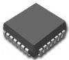
and CMOS drive levels. Available packages of A1010B include plastic
and ceramic J-leaded chip carriers, ceramic

 A1010B Data Sheet