Features: • High-impedance output during sleep mode
• Compatible with 2.5 to 3.5 V power supplies
• 10 mW power consumption in the active mode
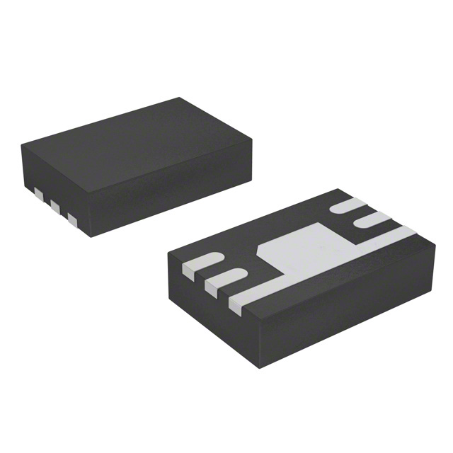
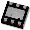
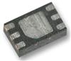
• Miniature MLP package
• Ratiometric output scales with the ratiometric supply reference voltage (VREF pin)
• Temperature-stable quiescent output voltage and sensitivity
• Wide ambient temperature range: 20°C to 85°C
• ESD protection greater than 3 kV
• Solid-state reliability
• Preset sensitivity and offset at final testSpecificationsSupply Voltage, VCC.......................................................8 V
Reverse-Supply Voltage, VRCC ................................0.1 V
Ratiometric Supply Reference Voltage, VREF .................7 V
Reverse-Ratiometric Supply
Reference Voltage, VRREF .....................................0.1 V
Logic Supply Voltage, VSLEEP (VCC > 2.5 V) ...............32 V
Reverse-Logic Supply Voltage, VRSLEEP .................0.1 V
Output Voltage, VOUT..................................... VCC + 0.1 V
Reverse-Output Voltage, VROUT..............................0.1 V
Temperatures
Operating Ambient, TA , Range S...............20ºC to 85ºC
Junction, TJ(MAX)......................................................165ºC
Storage, TS ............................................. 65ºC to 170ºCDescriptionThese linear Hall effect sensor integrated circuits (ICs) provide a voltage output that is directly proportional to an applied magnetic field. Before amplification, the sensitivity of typical Hall effect ICs (measured in mV/G) is directly proportional to the current flowing through the Hall effect transducer element inside the ICs. In many applications, it is difficult to achieve sufficient sensitivity levels with a Hall effect sensor IC without consuming more than 3 mA of current. The A1391 and A1392 minimize current consumption to less than 25 µA through the addition of a user-selectable sleep mode. This makes these devices perfect for battery-operated applications such as: cellular phones, digital cameras, and portable tools. End users can control the current consumption of the A1391 and A1392 by applying a logic level signal to the SLEEP pin. The outputs of the devices are not valid (high-impedance mode) during sleep mode. The high-impedance output feature allows the connection of multiple A1391 and A1392 Hall effect devices to a single A-to-D converter input.
The quiescent output voltage of A1392 is 50% nominal of the ratiometric supply reference voltage applied to the VREF pin of the device. The output voltage of the device is not ratiometric with respect to the SUPPLY pin.
Despite the low power consumption of the circuitry in the A1391 and A1392, the features required to produce a highly-accurate linear Hall effect IC have not been compromised. Each BiCMOS monolithic circuit integrates a Hall element, improved temperature-compensating circuitry to reduce the intrinsic sensitivity drift of the Hall element, a small-signal high-gain amplifier, and proprietary dynamic offset cancellation circuits. End of line, postpackaging, factory programming allows precise control of A1392 sensitivity and offset.
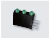
A1392 is available in a small 2.0 × 3.0 mm, 0.75 mm nominal height micro leaded package (MLP). It is Pb (lead) free, with 100% matte tin leadframe plating.

 A1392 Data Sheet