Features: Single power supply operation
- Full voltage range: 2.7 to 3.6 volt read and write operations for battery-powered applications
- Regulated voltage range: 3.0 to 3.6 volt read and write operations for compatibility with high performance 3.3 volt microprocessors
Access times:
- 70/90 (max.)
Current:
- 4 mA typical active read current
- 20 mA typical program/erase current
- 200 nA typical CMOS standby
- 200 nA Automatic Sleep Mode current
Flexible sector architecture
- 16 Kbyte/ 8 KbyteX2/ 32 Kbyte/ 64 KbyteX7 sectors
- Any combination of sectors can be erased
- Supports full chip erase
- Sector protection:
A hardware method of protecting sectors to prevent any inadvertent program or erase operations within that sector. Temporary Sector Unprotect feature allows code changes in previously locked sectors
Unlock Bypass Program Command
- Reduces overall programming time when issuing multiple program command sequence
Top or bottom boot block configurations available
Embedded Algorithms
- Embedded Erase algorithm will automatically erase the entire chip or any combination of designated sectors and verify the erased sectors
- Embedded Program algorithm automatically writes and verifies data at specified addresses
Typical 100,000 program/erase cycles per sector
20-year data retention at 125°C
- Reliable operation for the life of the system
Compatible with JEDEC-standards
- Pinout and software compatible with single-powersupply Flash memory standard
- Superior inadvertent write protection
Data Polling and toggle bits
- Provides a software method of detecting completion of program or erase operations
Ready / BUSY pin (RY / BY)
- Provides a hardware method of detecting completion of program or erase operations (not available on 32-pin PLCC & (s)TSOP packages)
Erase Suspend/Erase Resume
- Suspends a sector erase operation to read data from,or program data to, a non-erasing sector, then resumes the erase operation
Hardware reset pin (RESET )
- Hardware method to reset the device to reading array data (not available on 32 pin PLCC & (s)TSOP packages)
Package options
- 40-pin TSOP (forward type), 32-pin PLCC or (s)TSOP (forward type)
Pinout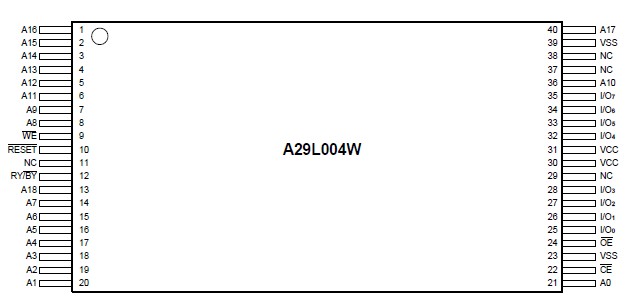 Specifications
Storage Temperature Plastic Packages . .. .0to + 70
Ambient Temperature with Power Applied.. 0 to + 70
Voltage with Respect to Ground
VCC (Note 1) . . . . . . . . . . . . . . . . . ..... . . -0.5V to +4.0V
A9, OE & RESET (Note 2) . . . . . . . . . . ... . -0.5 to +12.5V
All other pins (Note 1) . . . . . . . ... ... -0.5V to VCC + 0.5V
Output Short Circuit Current (Note 3) . . .. . . . . ... 200mA
Notes:
1. Minimum DC voltage on input or I/O pins is -0.5V. During voltage transitions, input or I/O pins may undershoot VSSto -2.0V for periods of up to 20ns. Maximum DC voltage on input and I/O pins is VCC +0.5V. During voltage transitions, input or I/O pins may overshoot to VCC +2.0V for periods up to 20ns.
2. Minimum DC input voltage on A9,OE and RESET is -0.5V. During voltage transitions, A9, OE and RESET may overshoot VSS to -2.0V for periods of up to 20ns.Maximum DC input voltage on A9 is +12.5V which may overshoot to 14.0V for periods up to 20ns. (RESET is N/A on 32-pin PLCC & (s)TSOP)
3. No more than one output is shorted at a time. Duration of the short circuit should not be greater than one second.
DescriptionThe A29L004 is a 4Mbit, 3.0 volt-only Flash memory organized as 524,288 bytes of 8 bits. The 8 bits of data appear on I/O0 - I/O7. The A29L004 is offered in 40-pin TSOP, 32-pin PLCC or (s)TSOP packages. This device A29L004 is designed to be programmed in-system with the standard system 3.0 volt VCC supply. Additional 12.0 volt VPP is not required for in-system write or erase operations. However,the A29L004 can also be programmed in standard EPROM programmers.
The A29L004 has the first toggle bit, I/O6, which indicates whether an Embedded Program or Erase is in progress, or it is in the Erase Suspend. Besides the I/O6 toggle bit, the A29L004 has a second toggle bit, I/O2, to indicate whether the addressed sector is being selected for erase. The A29L004 also offers the ability to program in the Erase Suspend mode. The standard A29L004 offers access times of 70 and 90ns, allowing high-speed microprocessors to operate without wait states. To e liminate bus contention the device has separate chip enable (CE ), write enable (WE ) and output enable (OE ) controls.
The device A29L004 requires only a single 3.0 volt power supply for both read and write functions. Internally generated and regulated voltages are provided for the program and erase operations.
The A29L004 is entirely software command set compatible with the JEDEC single-power-supply Flash standard.Commands are written to the command register using standard microprocessor write timings. Register contents serve as input to an internal state-machine that controls the erase and programming circuitry. Write cycles also internally latch addresses and data needed for the programming and erase operations. Reading data out of the device is similar to reading from other Flash or EPROM devices.
Device programming occurs by writing the proper program command sequence. This initiates the Embedded Program algorithm - an internal algorithm that automatically times the program pulse widths and verifies proper program margin.
Device erasure occurs by executing the proper erase command sequence. This initiates the Embedded Erase algorithm - an internal algorithm that automatically preprograms the array (if it is not already programmed)before executing the erase operation. During erase, the device automatically times the erase pulse widths and verifies proper erase margin. The Unlock Bypass mode facilitates faster programming times by requiring only two write cycles to program data instead of four.
The host system can detect whether a program or erase operation is complete by observing the RY / BY pin (not available on 32-pin PLCC & (s)TSOP), or by reading the I/O7 (Data Polling) and I/O6 (toggle) status bits. After a program or erase cycle has been completed, the device is ready to read array data or accept another command.The sector erase architecture allows memory sectors to be erased and reprogrammed without affecting the data contents of other sectors. The A29L004 is fully erased when shipped from the factory.
The hardware sector protection feature disables operations for both program and erase in any combination of the sectors of memory. This can be achieved via programming equipment.
The Erase Suspend/Erase Resume feature enables the user to put erase on hold for any period of time to read data from,or program data to, any other sector that is not selected for erasure. True background erase can thus be achieved.
The hardware RESET pin terminates any operation in progress and resets the internal state machine to reading array data (not available on 32-pin PLCC & (s)TSOP). The RESET pin may be tied to the system reset circuitry. A system reset would thus also reset the device, enabling the system microprocessor to read the boot-up firmware from the Flash memory.
The device A29L004 offers two power-saving features. When addresses have been stable for a specified amount of time,the device enters the automatic sleep mode. The system can also place the device into the standby mode. Power consumption is greatly reduced in both these modes.

 A29L004TX-90 Data Sheet