Features: The A29L040A is a 3.0 volt-only Flash memory organized as 524,288 bytes of 8 bits each. The 512 Kbytes of data are
further divided into eight sectors of 64 Kbytes each for flexible sector erase capability. The 8 bits of data appear on
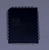
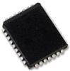
I/O0 - I/O7 while the addresses are input on A0 to A18. The A29L040A is offered in 32-pin PLCC, TSOP (8mm x 20mm) or sTSOP (8mm x 13.4mm) packages. This device is designed to be programmed in-system with the standard system 3.0 volt VCC supply. Additional 12.0 volt VPP is not required for in-system write or erase operations. However,
the A29L040A can also be programmed in standard EPROM programmers.
The A29L040A has a second toggle bit, I/O2, to indicate whether the addressed sector is being selected for erase,
and also offers the ability to program in the Erase Suspend mode. The standard A29L040A offers access times of 70ns, allowing high-speed microprocessors to operate without wait states. To eliminate bus contention the device has separate chip enable ( CE ), write enable (WE ) and output enable (OE ) controls.
The device requires only a single 3.0 volt power supply for both read and write functions. Internally generated and regulated voltages are provided for the program and erase operations.
The A29L040A is entirely software command set compatible with the JEDEC single-power-supply Flash standard.
Commands are written to the command register using standard microprocessor write timings. Register contents
serve as input to an internal state-machine that controls the erase and programming circuitry. Write cycles also internally latch addresses and data needed for the programming and erase operations. Reading data out of the device is similar to reading from other Flash or EPROM devices.
Device programming occurs by writing the proper program command sequence. This initiates the Embedded Program
algorithm - an internal algorithm that automatically times the program pulse widths and verifies proper program margin. Device erasure occurs by executing the proper erase command sequence. This initiates the Embedded Erase
algorithm - an internal algorithm that automatically preprograms the array (if it is not already programmed) before executing the erase operation. During erase, the device automatically times the erase pulse widths and verifies proper erase margin.
The host system can detect whether a program or erase operation is complete by reading the I/O7 (Data Polling) and I/O6 (toggle) status bits. After a program or erase cycle has been completed, the device is ready to read array data or accept another command.
The sector erase architecture allows memory sectors to be erased and reprogrammed without affecting the data.
SpecificationsStorage Temperature Plastic Packages . . . . . .0°C to + 70°C
. . . . . . . . . . . . . . . . . . . . . for -U series . . . . -40°C to +85°C
Ambient Temperature with Power Applied . . . 0°C to + 70°C
. . . . . . . . . . . . . . . . . . . . . . for -U series. . . . -40°C to +85°C
Voltage with Respect to Ground
VCC (Note 1) . . . . . . . . . . . . . . . . . . . . . . . . . . . -0.5V to +4.0V
A9 &OE (Note 2) . . . . . . . . . . . . . . . . . . . . . . . -0.5 to +12.5V
All other pins (Note 1) . . . . . . . . . . . . . . . .-0.5V to VCC + 0.5V
Output Short Circuit Current (Note 3) . . . . . . . . . . . . . . 200mA
DescriptionThe A29L040A is a 3.0 volt-only Flash memory organized as 524,288 bytes of 8 bits each. The 512 Kbytes of data are
further divided into eight sectors of 64 Kbytes each for flexible sector erase capability. The 8 bits of data appear on
I/O0 - I/O7 while the addresses are input on A0 to A18. The A29L040A is offered in 32-pin PLCC, TSOP (8mm x 20mm) or sTSOP (8mm x 13.4mm) packages. This device is designed to be programmed in-system with the standard system 3.0 volt VCC supply. Additional 12.0 volt VPP is not required for in-system write or erase operations. However,
the A29L040A can also be programmed in standard EPROM programmers.
The A29L040A has a second toggle bit, I/O2, to indicate whether the addressed sector is being selected for erase,
and also offers the ability to program in the Erase Suspend mode. The standard A29L040A offers access times of 70ns, allowing high-speed microprocessors to operate without wait states. To eliminate bus contention the device has separate chip enable ( CE ), write enable (WE ) and output enable (OE ) controls.
The device requires only a single 3.0 volt power supply for both read and write functions. Internally generated and regulated voltages are provided for the program and erase operations.
The A29L040A is entirely software command set compatible with the JEDEC single-power-supply Flash standard.
Commands are written to the command register using standard microprocessor write timings. Register contents
serve as input to an internal state-machine that controls the erase and programming circuitry. Write cycles also internally latch addresses and data needed for the programming and erase operations. Reading data out of the device is similar to reading from other Flash or EPROM devices.
Device A29L040A programming occurs by writing the proper program command sequence. This initiates the Embedded Program
algorithm - an internal algorithm that automatically times the program pulse widths and verifies proper program margin. Device erasure occurs by executing the proper erase command sequence. This initiates the Embedded Erase
algorithm - an internal algorithm that automatically preprograms the array (if it is not already programmed) before executing the erase operation. During erase, the device automatically times the erase pulse widths and verifies proper erase margin.
The host system can detect whether a program or erase operation is complete by reading the I/O7 (Data Polling) and I/O6 (toggle) status bits. After a program or erase cycle has been completed, the device is ready to read array data or accept another command.
The sector erase architecture allows memory sectors to be erased and reprogrammed without affecting the data contents of other sectors. The A29L040A is fully erased when shipped from the factory.
The hardware sector protection feature disables operations for both program and erase in any combination of the sectors of memory. This can be achieved via programming equipment.
The Erase Suspend feature enables the user to put erase on hold for any period of time to read data from, or program data to, any other sector that is not selected for erasure. True background erase can thus be achieved.
Power consumption is greatly reduced when the device is placed in the standby mode.

 A29L040A Data Sheet