Series: -
Number of Outputs: 1
Mounting Type: Surface Mount
Evaluation Tools: -
Packaging: Tube
Applications: Stepper Motor Driver, 2 Phase
Operating Temperature: -20°C ~ 85°C
Manufacturer: Allegro Microsystems Inc
Current - Output: ±650mA
Voltage - Load: 4.5 V ~ 30 V
Voltage - Supply: 4.75 V ~ 5.5 V
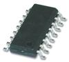
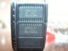
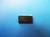
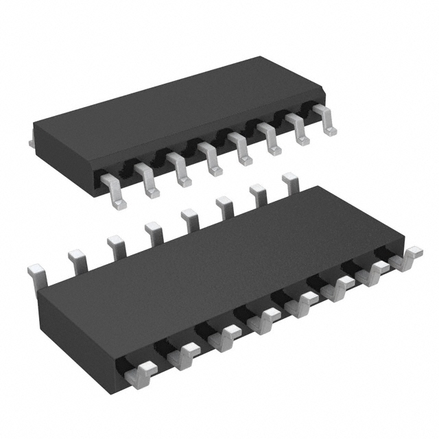
Package / Case: 16-SOIC (0.295", 7.50mm Width)
Supplier Device Package: 16-SOIC W
Features: ±650 mA Continuous Output Current
30 V Output Voltage Rating
Internal Fixed-Frequency PWM Current Control
Satlington Sink Drivers
User-Selectable Blanking Window
Internal Ground-Clamp & Flyback Diodes
Internal Thermal-Shutdown Circuitry
Crossover-Current Protection and UVLO ProtectionPinout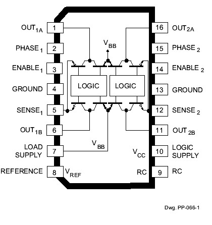 Specifications
Load Supply Voltage, VBB ....................... 30 V
Output Current, IOUT (peak) ........... ±750 mA
(continuous) .................................... ±650 mA
Logic Supply Voltage, VCC ...................... 7.0 V
Input Voltage, Vin ......... -0.3 V to VCC + 0.3 V
Sense Voltage, VS ................................. 1.0 V
Package Power Dissipation (TA = 25°C), PD
A3966SA .......................................... 2.08 W*
A3966SLB ........................................ 1.87 W*
Operating Temperature Range,
TA ..................................... -20°C to +85°C
Junction Temperature,
TJ ................................................... +150°C
Storage Temperature Range,
TS ................................... -55°C to +150°C
Output current rating may be limited by duty cycle, ambient temperature, and heat sinking. Under any set of conditions, do not exceed the specified current rating or a junction temperature of 150°C.
* Per SEMI G42-88 Specification, Thermal Test Board Standardization for Measuring Junction-to-Ambient Thermal Resistance of Semiconductor Packages.
DescriptionThe A3966SA and A3966SLB are designed to drive both windings of a twophase bipolar stepper motor. Each device includes two H-bridges capable of continuous output currents of ±650 mA and operating voltages to 30 V. Motor winding current can be controlled by the internal fixed-frequency, pulse-width modulated (PWM), current-control circuitry. The peak load current limit is set by the user's selection of a reference voltage and current-sensing resistors. Except for package style and pinout, the two devices are identical.
The fixed-frequency pulse duration is set by a user-selected external RC timing network. The capacitor in the RC timing network also determines a userselectable blanking window that prevents false triggering of the PWM currentcontrol circuitry during switching transitions.
To reduce on-chip power dissipation, the H-bridge power outputs have been optimized for low saturation voltages. The sink drivers feature the Allegro® patented Satlington® output structure. The Satlington outputs combine the low voltage drop of a saturated transistor and the high peak current capability of a Darlington.
For each bridge, a PHASE input controls load-current polarity by selecting the appropriate source and sink driver pair. For each bridge, an ENABLE input, when held high, disables the output drivers. Special power-up sequencing is not required. Internal circuit protection includes thermal shutdown with hysteresis, ground-clamp and flyback diodes, and crossover-current protection.
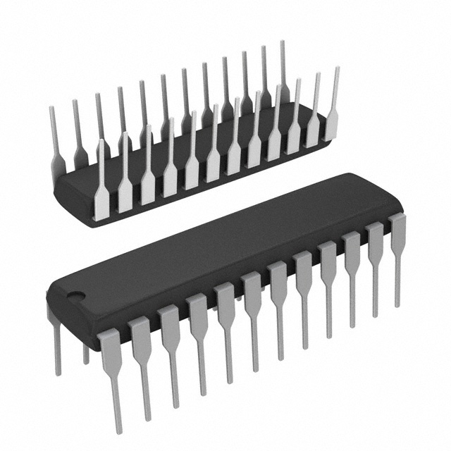
The A3966SA is supplied in a 16-pin dual in-line plastic package. The A3966SLB is supplied in a 16-lead plastic SOIC with copper heat sink tabs. The power tab is at ground potential and needs no electrical isolation. The A3966SLB is also available in a lead (Pb) free version, with 100% matte tin leadframe plating.
Parameters: | Technical/Catalog Information | A3966SLB |
| Vendor | Allegro Microsystems Inc |
| Category | Integrated Circuits (ICs) |
| Applications | Stepper Motor Driver, 2 Phase |
| Number of Outputs | 1 |
| Voltage - Supply | 4.75 V ~ 5.5 V |
| Voltage - Load | 4.5 V ~ 30 V |
| Current - Output | ±650mA |
| Operating Temperature | -20°C ~ 85°C |
| Package / Case | 16-SOIC |
| Packaging | Tube |
| Lead Free Status | Contains Lead |
| RoHS Status | RoHS Non-Compliant |
| Other Names | A3966SLB
A3966SLB
|
 A3966SLB Data Sheet