Series: -
Number of Outputs: 1
Evaluation Tools: -
Packaging: Tube
Applications: Stepper Motor Driver
Mounting Type: Through Hole
Current - Output: ±1.5A
Voltage - Supply: 4.5 V ~ 5.5 V
Operating Temperature: -20°C ~ 85°C
Manufacturer: Allegro Microsystems Inc
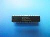
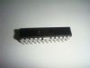
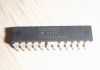
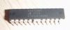
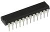
Package / Case: 24-DIP (0.300", 7.62mm)
Supplier Device Package: 24-DIP
Voltage - Load: 15 V ~ 50 V
Features: ±1.5 A, 50 V Continuous Output Rating
Low rDS(on) DMOS Output Drivers
Optimized Microstepping via 6-Bit Linear DACs
Programmable Mixed, Fast, and Slow Current-Decay Modes
4 MHz Internal Oscillator for Digital Timing
Serial-Interface Controls Chip Functions
Synchronous Rectification for Low Power Dissipation
Internal UVLO and Thermal Shutdown Circuitry
Crossover-Current Protection
Precision 2 V Reference
Inputs Compatible with 3.3 V or 5 V Control Signals
Sleep and Idle ModesPinout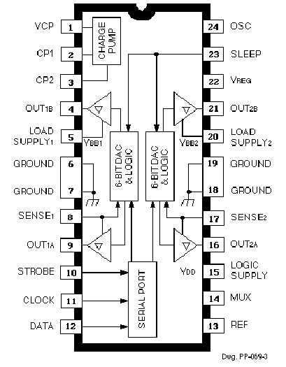 SpecificationsLoad Supply Voltage, VBB ................ 50 V
Output Current, IOUT.................... ±1.5 A
Logic Supply Voltage, VDD................ 7.0 V
Logic Input Voltage Range,
VIN .......................... -0.3 V to VDD + 0.3 V
Reference Voltage, VREF ..................... 3 V
Sense Voltage (dc), VS ................. 500 mV
Package Power Dissipation,
PD ................................................... 3.1 W
Operating Temperature Range,
TA ................................. -20°C to +85°C
Junction Temperature, TJ ........... +150°C
Storage Temperature Range,
TS ............................... -55°C to +150°C
Output current rating may be limited by duty cycle, ambient temperature, and heat sinking. Under any set of conditions, do not exceed the specified current rating or a junction temperature of 150°C.DescriptionThe A3972SB is designed as dual DMOS full bridge microstepping PWM motor driver for pulse-width modulated (PWM) current control of bipolar microstepping stepper motors. It is capable of continuous output currents to ±1.5 A and operating voltages to 50 V. Internal fixed off-time PWM current-control timing circuitry can be programmed via a serial interface to operate in slow, fast, and mixed current-decay modes.
A3972SB has twelve features. (1) ±1.5A, 50V continuous output rating. (2) Low rDS(on) DMOS output drivers. (3) Optimized microstepping via 6-bit linear DACs. (4) Programmable mixed, fast, and slow current-decay modes. (5) 4MHz internal oscillator for digital timing. (6) Serial-interface controls chip functions. (7) Synchronous rectification for low power dissipation. (8) Internal UVLO and thermal shutdown circuitry. (9) Crossover current protection. (10) Precision 2V reference. (11) Inputs compatible with 3.3V or 5V control signals. (12) Sleep and idle modes. That are all the main features.
Some absolute maximum ratings of A3972SB have been concluded into several points as follow. (1) Its load supply voltage would be 50V. (2) Its output current would be +/-1.5A. (3) Its logic supply voltage would be 7.0V. (4) Its logic input voltage range would be from -0.3V to Vdd+0.3V. (5) Its reference voltage would be 3V. (6) Its sense voltage dc would be 500mV. (7) Its package power dissipation would be 3.1W. (8) Its operating temperature range would be from -20°C to +85°C. (9) Its junction temperature range would be from +150°C. (10) Its storage temperature range would be from -55°C to +150°C. It should be noted that output current rating may be limited by duty cycle, ambient temperature, and heat sinking. Under any set of conditions, do not exceed the specified current rating or a junction temperature of 150°C. And so on. If you have any question or suggestion or want to know more information please contact us for details. Thank you!
Parameters: | Technical/Catalog Information | A3972SB |
| Vendor | Allegro Microsystems Inc |
| Category | Integrated Circuits (ICs) |
| Applications | Stepper Motor Driver |
| Number of Outputs | 1 |
| Voltage - Supply | 4.5 V ~ 5.5 V |
| Voltage - Load | 15 V ~ 50 V |
| Current - Output | ±1.5A |
| Operating Temperature | -20°C ~ 85°C |
| Package / Case | 24-DIP |
| Packaging | Tube |
| Lead Free Status | Contains Lead |
| RoHS Status | RoHS Non-Compliant |
| Other Names | A3972SB
A3972SB
|
 A3972SB Data Sheet