A49LF040A

Features: • Single Power Supply Operation- Low voltage range: 3.0 V - 3.6 V for Read and Write Operations• Standard Intel Low Pin Count Interface- Read compatible to Intel® Low Pin Count (LPC) interface• Memory Configuration- 512K x 8 (4 Mbit)• Block Architecture- 4Mbit...

product image

A49LF040A Picture
SeekIC No. : 004260366 Detail

A49LF040A: Features: • Single Power Supply Operation- Low voltage range: 3.0 V - 3.6 V for Read and Write Operations• Standard Intel Low Pin Count Interface- Read compatible to Intel® Low Pin C...

floor Price/Ceiling Price

Part Number:
A49LF040A
Supply Ability:
5000

Price Break

  • Qty
  • 1~5000
  • Unit Price
  • Negotiable
  • Processing time
  • 15 Days
Total Cost: $ 0.00

SeekIC Buyer Protection PLUS - newly updated for 2013!

  • Escrow Protection.
  • Guaranteed refunds.
  • Secure payments.
  • Learn more >>

Month Sales

268 Transactions

Rating

evaluate  (4.8 stars)

Upload time: 2024/4/28

Payment Methods

All payment methods are secure and covered by SeekIC Buyer Protection PLUS.

Notice: When you place an order, your payment is made to SeekIC and not to your seller. SeekIC only pays the seller after confirming you have received your order. We will also never share your payment details with your seller.
Product Details

Description


Features:

• Single Power Supply Operation
- Low voltage range: 3.0 V - 3.6 V for Read and Write Operations
• Standard Intel Low Pin Count Interface
- Read compatible to Intel® Low Pin Count (LPC) interface
• Memory Configuration
- 512K x 8 (4 Mbit)
• Block Architecture
- 4Mbit: eight uniform 64KByte blocks
- Supports full chip erase for Address/Address
Multiplexed (A/A Mux) mode
• Automatic Erase and Program Operation
- Embedded Byte Program and Block/Chip Erase algorithms
- Typical 10 s/byte programming time
- Typical 1s block erase time
• Two Operational Modes
- Low Pin Count Interface (LPC) Mode for in-system operation
- Address/Address Multiplexed (A/A Mux) Interface
Mode for programming equipment
• Low Pin Count (LPC) Mode
- 33 MHz synchronous operation with PCI bus
- 5-signal communication interface for in-system read
and write operations
- Standard SDP Command Set
- Data Polling (I/O7) and Toggle Bit (I/O6) features
- Block Locking Register for all blocks
- 4 ID pins for multi-chip selection
- 5 GPI pins for General Purpose Input Register
- TBL pin for hardware write protection to Boot Block
- WP pin for hardware write protection to whole
memory array except Boot Block
• Address/Address Multiplexed (A/A Mux) Mode
- 11-pin multiplexed address and 8-pin data I/O interface
- Supports fast programming on EPROM programmers
- Standard SDP Command Set
- Data Polling (I/O7) and Toggle Bit (I/O6) features
• Lower Power Consumption
- Typical 12mA active read current
- Typical 24mA program/erase current
• High Product Endurance
- Guarantee 100,000 program/erase cycles for each block
- Minimum 20 years data retention
• Compatible Pin-out and Packaging
- 32-pin (8 mm x 14 mm) TSOP (TYPE I)
- 32-pin PLCC
- Optional Pb-free (Lead-free) package
- All Pb-free (Lead-free) products are RoHS compliant


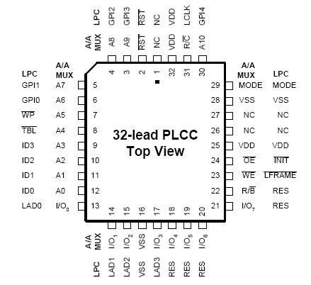
Pinout

  Connection Diagram


Specifications

Temperature Under Bias . . . . . . . . . . .. . . . . . . . -55°C to + 125°C
Storage Temperature . . . . . . . . . . . . ... . . . . . . . -65°C to + 125°C
D.C. Voltage on Any Pins with Respect to Ground (1)
. . . . . . . . . . . . . . . . . . . . . . . . . ... . . .. . . . . . . -0.5V to VDD + 0.5V
Package Power Dissipation Capability (Ta=25°C)
. . . . . . . . . . . . . . . . . . . . . . . . .. . .. . . . . .. . -0.5V to VDD + 0.5V
Output Short Circuit Current (2) . . . . . . .. . . . . .. . . . . . . . . . 50mA
Notes:
1. Minimum DC voltage on input or I/O pins is -0.5V. During voltage
transitions, input or I/O pins may undershoot VSS to -2.0V for
periods of up to 20ns. Maximum DC voltage on input and I/O
pins is VDD + 0.5V. During voltage transitions, input or I/O pins
may overshoot to VDD + 2.0V for periods up to 20ns.
2. No more than one output is shorted at a time. Duration of the
short circuit should not be greater than one second.


Description

The A49LF040A flash memory device is designed to be read-compatible with the Intel Low Pin Count (LPC) Interface Specification 1.1. This device is designed to use a single low voltage, range from 3.0 Volt to 3.6 Volt power supply to perform in-system or off-system read and write operations. It provides protection for the storage and update of code and data in addition to adding system design flexibility through five general-purpose inputs. Two interface modes are supported by the A49LF040A: Low Pin Count (LPC) Interface mode for In-System programming and Address/Address Multiplexed (A/A Mux) mode for fast factory programming of PC-BIOS applications.

The memory is divided into eight uniform 64Kbyte blocks that can be erased independently without affecting the data in other blocks. Blocks also can be protected individually to prevent accidental Program or Erase commands from modifying the memory. The boot block can be write protected by a hardware method controlled by the TBL pin or a register-based protection turned on/off by the Block Locking Registers (LPC mode only). The rest of blocks except boot block in the device also can be write protected by WP pin or
Block Locking Registers (LPC mode only). The Program and Erase operations are executed by issuing the Program/Erase commands into the command interface by which activating
the internal control logic to automatically process the Program/Erase procedures. The device can be programmed on a byte-by-byte basis after performing the Erase operation.

In addition to the Block Erase operation, the Chip Erase feature is provided in A/A Mux mode that allows the whole memory to be erased in one single Erase operation. The A49LF040A provides the status detection such as Data Polling (I/O7) and Toggle Bit (I/O6) Functions in both FWH/LPC and A/A Mux modes. The process or completion of Program and Erase operations can be detected by reading the status bits.

The A49LF040A is offered in 32-lead TSOP and 32-lead PLCC packages with optional environmental friendly leadfree package. See Figures 1 and 2 for pin assignments and Table 1 for pin descriptions.


Customers Who Bought This Item Also Bought

Margin,quality,low-cost products with low minimum orders. Secure your online payments with SeekIC Buyer Protection.
Crystals and Oscillators
Motors, Solenoids, Driver Boards/Modules
Memory Cards, Modules
Optical Inspection Equipment
Discrete Semiconductor Products
View more