Features: • 66 MHz PCI
• CPLD and FPGA Integration
• Single Chip Solution
• 100% Resource Utilization with 100% Pin Locking
• 3.3V Operation with 5.0V Input Tolerance
• Very Low Power Consumption
• Deterministic, User-Controllable Timing
• Unique In-System Diagnostic and Debug capability with Silicon Explorer II
• Boundary Scan Testing in Compliance with IEEE Standard 1149.1 (JTAG)
• Secure Programming Technology Prevents Reverse Engineering and Design TheftApplication• 12,000 to 48,000 System Gates
• Up to 249 User-Programmable I/O Pins
• Up to 1080 Flip-Flops
• 0.35µ CMOSPinout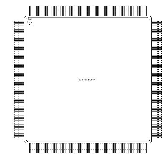 Specifications
| Symbol Parameter Limits Units |
| VCCR2 DC Supply Voltage3 0.3 to +6.0 V |
| VCCA2 DC Supply Voltage 0.3 to +4.0 V |
VCCI2
DC Supply Voltage
(A54SX08, A54SX16,A54SX32)
0.3 to +4.0 V |
VCCI2 DC Supply Voltage
(A54SX16P) 0.3 to +6.0 V |
| VI Input Voltage 0.5 to +5.5 V |
| VO Output Voltage 0.5 to +3.6 V |
IIO I/O Source Sink
Current3 30 to +5.0 mA |
| TSTG Storage Temperature 65 to +150 °C |
Notes:
1. Stresses beyond those listed under "Absolute Maximum Ratings" may cause permanent damage to the device. Exposure to absolute maximum rated conditions for extended periods may affect device reliability. Device should not be operated outside the Recommended Operating Conditions.
2. VCCR in the A54SX16P must be greater than or equal to VCCI during power-up and power-down sequences and during normal operation.
3. Device inputs are normally high impedance and draw extremely low current. However, when input voltage is greater than VCC + 0.5V or less than GND 0.5V, the internal protection diodes will forward-bias and can draw excessive current.
DescriptionActel's SX family of FPGAs features a sea-of-modules architecture that delivers device performance and integration levels not currently achieved by any other FPGA architecture. SX devices greatly simplify design time, enable dramatic reductions in design costs and power consumption, and further decrease time to market for performance-intensive applications.
Actel's SX architecture features two types of logic modules, the combinatorial cell (C-cell) and the register cell (R-cell), each optimized for fast and efficient mapping of synthesized logic functions. The routing and interconnect resources are in the metal layers above the logic modules, providing optimal use of silicon. This enables the entire floor of the device to be spanned with an uninterrupted grid of fine-grained, synthesis-friendly logic modules (or "sea-of-modules"), which reduces the distance signals have to travel between logic modules. To minimize signal propagation delay, SX devices employ both local and general routing resources. The high-speed local routing resources (DirectConnect and FastConnect) enable very fast local signal propagation that is optimal for fast counters, state machines, and datapath logic. The general system of segmented routing tracks allows any logic module in the array to be connected to any other logic or I/O module. Within this system, propagation delay is minimized by limiting the number of antifuse interconnect elements to five (90 percent of connections typically use only three antifuses). The unique local and general routing structure featured in SX devices gives fast and predictable performance, allows 100 percent pin-locking with full logic utilization, enables concurrent PCB development, reduces design time, and allows designers to achieve performance goals with minimum effort.
Further complementing SX's flexible routing structure is a hard-wired, constantly loaded clock network that has been tuned to provide fast clock propagation with minimal clock skew. Additionally, the high performance of the internal logic has eliminated the need to embed latches or flip-flops in the I/O cells to achieve fast clock-to-out or fast input set-up times. SX devices have easy-to-use I/O cells that do not require HDL instantiation, facilitating design re-use and reducing design and verification time.

 A54SX08 Data Sheet