Features: ·Fast access times: 4.2/4.5/5.0 ns (143/133/100 MHZ)
·Single +3.3V+10% or +3.3V-5% power supply
·Synchronous burst function
·Individual Byte Write control and Global Write
·Registered output for pipelined applications
·Three separate chip enables allow wide range of options for CE control, address pipelining
·Selectable BURST mode
·SLEEP mode (ZZ pin) provided
·Available in 100-pin LQFP packagePinout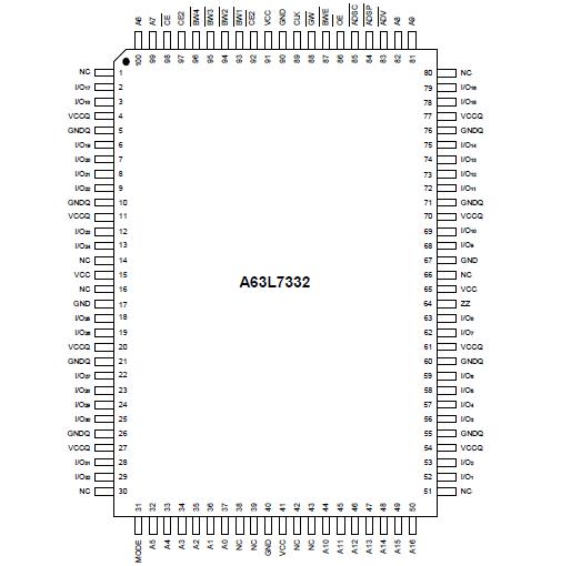 SpecificationsPower Supply Voltage (VCC) . . . . . . -0.5V to +4.6V
Voltage Relative to GND for any Pin Except VCC (Vin,
Vout) . . . . . . . . . . . . . . . . . . . . . -0.5V to VCC +0.5V
Power Dissipation (PD) . . . . . . . . . . . . . . . . . . . . 2W
Operating Temperature (Topr) . . . . . . 0°C to 70°C
Storage Temperature (Tbias) . . . . . -10°C to 85 °C
Storage Temperature (Tstg) . . . . . -55°C to 125°CDescriptionThe A63L7332 is a high-speed, low-power SRAM containing 4,194,304 bits of bit synchronous memory, organized as 131,072 words by 32 bits.
The A63L7332 combines advanced synchronous peripheral circuitry, 2-bit burst control, input registers, output registers and a 128K X 32 SRAM core to provide a wide range of data RAM applications.
The positive edge triggered single clock input (CLK) of A63L7332 controls all synchronous inputs passing through the registers. Synchronous inputs include all addresses (A0 - A16), all data inputs (I/O1 - I/O36), active LOW chip enable ( CE ), two additional chip enables (CE2, CE2 ), burst control inputs ( ADSC , ADSP , ADV ), byte write enables ( BWE , BW1 , BW2 , BW3 , BW4 ) and Global Write (GW ). Asynchronous inputs include output enable ( OE ), clock (CLK), BURST mode (MODE) and SLEEP mode (ZZ).
Burst operations can be initiated with either the address status processor ( ADSP ) or address status controller ( ADSC ) input pin. Subsequent burst sequence burst addresses can be internally generated by the A63P7336 and controlled by the burst advance ( ADV ) pin. Write cycles are internally self-timed and synchronous with the rising edge of the clock (CLK).
This feature of A63L7332 simplifies the write interface. Individual Byte enables allow individual bytes to be written. BW1 controls I/O1 - I/O9, BW2 controls I/O10 - I/O18, BW3 controls I/O19 - I/O27, and BW4 controls I/O28 - I/O36, all on the condition thatBWE is LOW. GW LOW causes all bytes to be written.

 A63L7332 Data Sheet


