Features: ·Fast access time: 4.5/5.0/6.0 ns (117/100/83MHz)
·Direct Bus Alternation between READ and WRITE cycles allows 100% bus utilization
·Signal +3.3V ± 5% power supply
·Individual Byte Write control capability
·Clock enable (CEN) pin to enable clock and suspend operations
·Clock-controlled and registered address, data and control signals
·Registered output for pipelined applications
·Three separate chip enables allow wide range of options for CE control, address pipelining
·Internally self-timed write cycle
·Selectable BURST mode (Linear or Interleaved)
·SLEEP mode (ZZ pin) provided
·Available in 100 pin LQFP packagePinout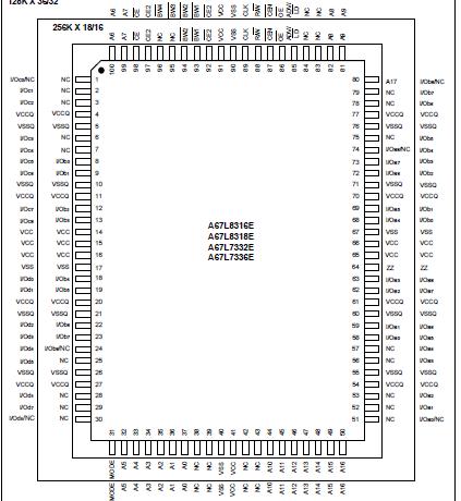 SpecificationsPower Supply Voltage (VCC) . . . . . . . -0.5V to +4.6V
Voltage Relative to GND for any Pin Except VCC (Vin,
Vout) . . . . . . . . . . . . . . . . . . . . . .-0.5V to VCC+0.5V
Operating Temperature (Topr) . . . . . 0°C to 70°C
Storage Temperature (Tbias) . . . . -10°C to 85 °C
Storage Temperature (Tstg) . . . . . -55°C to 125°CDescriptionThe AMIC Zero Bus Latency (ZeBLTM) SRAM family employs high-speed, low-power CMOS designs using an advanced CMOS process.
A67L8316, A67L8318, A67L7332, A67L7336 SRAMs integrate a 256K X 16, 256K X 18, 128K X 32 or 128K X 36 SRAM core with advanced synchronous peripheral circuitry and a 2-bit burst counter. These SRAMs are optimized for 100 percent bus utilization without the insertion of any wait cycles during Write-Read alternation. The positive edge triggered single clock input (CLK) controls all synchronous inputs passing through the registers.The positive edge triggered single clock input (CLK) controls all synchronous inputs passing through the registers. The synchronous inputs include all address, all data inputs, active low chip enable (CE), two additional chip enables for easy depth expansion (CE2, CE2), cycle start input (ADV/ LD ), synchronous clock enable ( CEN), byte write enables ( BW1 , BW2 , BW3 , BW4 ) and read/write (R/W).
Asynchronous inputs include the output enable (OE), clock (CLK), SLEEP mode (ZZ, tied LOW if unused) and burst mode (MODE). Burst Mode can provide either interleaved or linear operation, burst operation can be initiated by synchronous address Advance/Load (ADV/LD) pin in Low state. Subsequent burst address can be internally generated by the chip and controlled by the same input pin ADV/LD in High state.
Write cycles are internally self-time and synchronous with the rising edge of the clock input and when R/W is Low. The feature simplified the write interface. Individual Byte enables allow individual bytes to be written. BW1 controls I/Oa pins; BW2 controls I/Ob pins; BW3 controls I/Oc pins; and BW4 controls I/Od pins. Cycle types can only be defined when an address is loaded.
The A67L8316, A67L8318, A67L7332, A67L7336 SRAM operates from a +3.3V power supply, and all inputs and outputs are LVTTL-compatible. The device is ideally suited for high bandwidth utilization systems.

 A67L7336 Data Sheet