A67P8318

Features: •Fast access time: 2.6/2.8/3.2/3.5/3.8/4.2 (250/227/200/166/150/133MHz)•Zero Bus Latency between READ and WRITE cycles allows 100% bus utilization•Signal +2.5V ± 5% power supply•Individual Byte Write control capability•Clock enable (CEN) pin to enable clock ...

product image

A67P8318 Picture
SeekIC No. : 004260541 Detail

A67P8318: Features: •Fast access time: 2.6/2.8/3.2/3.5/3.8/4.2 (250/227/200/166/150/133MHz)•Zero Bus Latency between READ and WRITE cycles allows 100% bus utilization•Signal +2.5V ± 5% power...

floor Price/Ceiling Price

Part Number:
A67P8318
Supply Ability:
5000

Price Break

  • Qty
  • 1~5000
  • Unit Price
  • Negotiable
  • Processing time
  • 15 Days
Total Cost: $ 0.00

SeekIC Buyer Protection PLUS - newly updated for 2013!

  • Escrow Protection.
  • Guaranteed refunds.
  • Secure payments.
  • Learn more >>

Month Sales

268 Transactions

Rating

evaluate  (4.8 stars)

Upload time: 2024/5/7

Payment Methods

All payment methods are secure and covered by SeekIC Buyer Protection PLUS.

Notice: When you place an order, your payment is made to SeekIC and not to your seller. SeekIC only pays the seller after confirming you have received your order. We will also never share your payment details with your seller.
Product Details

Description


Features:

Fast access time: 2.6/2.8/3.2/3.5/3.8/4.2 (250/227/200/166/150/133MHz)
Zero Bus Latency between READ and WRITE cycles allows 100% bus utilization
Signal +2.5V ± 5% power supply
Individual Byte Write control capability
Clock enable (CEN) pin to enable clock and suspend operations


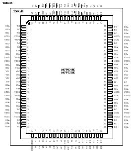
Pinout

  Connection Diagram


Specifications

Power Supply Voltage (VCC) . . . . . . . . . . -0.3V to +3.6V
Voltage Relative to GND for any Pin Except VCC (Vin,
Vout) . . . . . . . . . . . . . . . . . . . . . . . . -0.3V to VCC +0.3V
Operating Temperature (Topr) . . . . . . . . . 0°C to 70°C
Storage Temperature (Tbias) . . . . . . . . -10°C to 85 °C
Storage Temperature (Tstg) . . . . . . . . -55°C to 125°C
*Comments
Stresses above those listed under "Absolute Maximum Ratings" may cause permanent damage to this device. These are stress ratings only. Functional operation of this device at these or any other conditions above those indicated in the operational sections of this specification is not implied or intended. Exposure to the absolute maximum rating conditions for extended periods may affect device reliability.


Description

The AMIC Zero Bus Latency (ZeBLTM) SRAM family employs high-speed, low-power CMOS designs using an advanced CMOS process.

The A67P8318, A67P7336 SRAMs integrate a 256K X 18, 128K X 36 SRAM core with advanced synchronous peripheral circuitry and a 2-bit burst counter.

These SRAMs are optimized for 100 percent bus utilization without the insertion of any wait cycles during Write-Read alternation. The positive edge triggered single clock input (CLK) controls all synchronous inputs passing through the registers. The synchronous inputs include all address, all data inputs, active low chip enable (CE), two additional chip enables for easy depth expansion (CE2, CE2 ), cycle start input (ADV/ LD ), synchronous clock enable ( CEN), byte write enables (BW1,BW2,BW3,BW4) and read/write (R/W).

Asynchronous inputs include the output enable (OE), clock (CLK), SLEEP mode (ZZ, tied LOW if unused) and burst mode (MODE). Burst Mode can provide either interleaved or linear operation, burst operation can be initiated by synchronous address Advance/Load (ADV/LD) pin in Low state. Subsequent burst address can be internally generated by the chip and controlled by the same input pin ADV/LD in High state. Write cycles are internally self-time and synchronous with the rising edge of the clock input and when R/W is Low.

The feature of A67P8318, A67P7336 simplified the write interface. Individual Byte enables allow individual bytes to be written. BW1 controls I/Oa pins; BW2 controls I/Ob pins; BW3 controls I/Oc pins; and BW4 controls I/Od pins. Cycle types can only be defined when an address is loaded. The SRAM operates from a +2.5V power supply, and all inputs and outputs are LVTTL-compatible. The device is ideally suited for high bandwidth utilization systems.


Customers Who Bought This Item Also Bought

Margin,quality,low-cost products with low minimum orders. Secure your online payments with SeekIC Buyer Protection.