Features: • VIN Range: 2.7V to 5.5V• 150mA of Output Current- Peak Current up to 250mA• Regulated Output Voltage• 1.2MHz Switching Frequency• Low Noise Constant Frequency Operation• <1.0µA of Shutdown Current• Automatic Soft Start• Small App...
AAT3119: Features: • VIN Range: 2.7V to 5.5V• 150mA of Output Current- Peak Current up to 250mA• Regulated Output Voltage• 1.2MHz Switching Frequency• Low Noise Constant Frequen...
SeekIC Buyer Protection PLUS - newly updated for 2013!
268 Transactions
All payment methods are secure and covered by SeekIC Buyer Protection PLUS.

|
Symbol |
Description |
Value |
Units |
| VIN VOUT VEN VEN(MAX) IOUT TJ TLEAD |
Input Voltage Charge Pump Output EN to GND Voltage Maximum EN to Input Voltage Maximum DC Output Current Operating Junction Temperature Range Maximum Soldering Temperature (at leads, 10 sec) |
-0.3 to 6.0 -0.3 to 6.0 -0.3 to 6.0 0.3 250 -40 to 150 300 |
V V V V mA °C °C |
The AAT3119 is a general purpose high efficiency voltage regulated charge pump IC that can produce output current levels up to 150mA. As a voltage regulated output device, it may be used for general voltage boost applications or to power white, RGB, or flash type LEDs from a 2.7V to 5.5V input.
The voltage doubling charge pump architecture of the AAT3119 provides for a low external part count; just three small ceramic capacitors are needed. This makes the AAT3119 ideally suited for small battery-powered applications. This device operates from a fixed high frequency 1.2MHz oscillator which enables the use of very small external capacitors, one 1µF flying capacitor, and two 1µF bypass capacitors at IN and OUT.
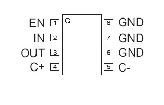
The AAT3119 has built-in soft-start circuitry which prevents excessive inrush current from the source supply during startup. A low-current shutdown feature disconnects the load from VIN and reduces quiescent current to less than 1.0µA when the device is disabled. The AAT3119 is available in a Pb-free, 8-pin SC70JW package and is rated over the -40°C to +85°C temperature range.