Features: ·Full Window Comparator
·2.0 pF max Input Capacitance
·9 V max Differential Input Voltage
·2.5 ns Propagation Delays
·Low Dispersion
·Low Input Bias Current
·Independent Latch Function
·Input Inhibit Mode
·80 dB CMRRApplication·High Speed Pin Electronic Receiver
·High Speed Triggers
·Threshold Detectors
·Peak DetectorsSpecificationsPower Supply Voltage
+VS to GND . . . . . . . . . . . . . . . . . . . . . . . . . . . . . +12 V
VS to GND . . . . . . . . . . . . . . . . . . . . . . . . . . . . . 9 V
Difference from +VS to VS . . . . . . . . . . . . . . . . . +16 V
Inputs
VINA/B, VINA, VINB . . . . . . .+VS 13.5 V, VS + 13.7 V
LEA, LEA, LEB, LEB . . . . . . . . . . +VS 14 V, VS + 12 V
IE, IE . . . . . . . . . . . . . . . . . . +VS 14 V, VS + 10.3 V
Outputs2
QA, QA, QB, QB . . . . . . . . . . GND 0.5 V, GND + 3.5 V
Operating Temperature Range . . . . . . . 0°C to +70°C
Storage Temperature Range
After Soldering . . . . . . . . . . . . . . . .65°C to + 125°C
Lead Temperature Range (Soldering 20 sec)3 ..+300°C
NOTES
1 Stresses above those limits under Absolute Maximum Ratings may cause permanent damage to the device. This is a stress rating only; functional operation of the device at these or any other conditions above those indicated in the operational sections of this specification is not implied. Exposure to absolute maximum rating conditions for extended periods may affect device reliability.
2 Limits apply for shorted output.
3 To ensure lead coplanarity (±0.002 inches) and solderability, handling with bare hands should be avoided and the device should be stored in an environment at 24°C ±5°C (75°F ±10°F) with relative humidity not to exceed 65%.
DescriptionThe AD1317 is an ultrahigh speed window comparator with a latch. It uses a high speed monolithic process to provide high dc accuracy without sacrificing input voltage range. The AD1317 guarantees a 2.8 ns maximum propagation delay.
On-chip connection of the common input eliminates the contributions of a second bonding pad and package pin to the input capacitance, resulting in a maximum input capacitance of 2 pF.The dispersion, or variation in propagation delay with input overdrive levels and slew rates, is typically 350 ps for 5 V signals and 200 ps for 1 V inputs.
The AD1317 employs a high precision differential input stage with a common-mode range of 9 V. Its complementary digital outputs are ECL compatible. The output stage is capable of driving a 50 W line terminated to 2 V. The AD1317 also provides a latch function, allowing operation in a sample-hold mode. The latch inputs can also be used to generate hysteresis.
The comparator input can be switched into a high impedance state through the inhibit mode feature, electrically removing the comparator from the circuit. The bias current in inhibit mode is typically 50 pA.
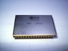
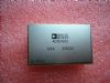
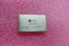
The AD1317 is available in a small 16-lead, hermetically sealed "gull-wing" surface mount package and operates over the commercial temperature range, 0°C to +70°C.

 AD1317 Data Sheet