Features: AD1555
`Fourth Order Modulator
`Large Dynamic Range
116 dB Min, 120 dB Typical @ 1 ms
117 dB Typical @ 0.5 ms
`Low Input Noise: 80 nV rms @ 4 ms with
Gain of 34,128
`Low Distortion: 111 dB Max, 120 dB Typical
`Low Intermodulation: 122 dB
`Sampling Rate at 256 kSPS
`Very High Jitter Tolerance
`No External Antialias Filter Required
`Programmable Gain Front End
`Input Range: ±2.25 V
`Robust Inputs
`Gain Settings: 1, 2.5, 8.5, 34, 128
`Common-Mode Rejection (DC to 1 kHz)
93 dB Min, 101 dB Typical @ Gain of 1
`77 mW Typical Low Power Dissipation
`Standby Modes
AD1556
`FIR Digital Filter/Decimator
`Serial or Parallel Selection of Configuration
`Output Word Rates: 250 SPS to 16 kSPS
`6.2 mW Typ Low Power Dissipation
`70 mW in Standby Mode
`Reference Design and Evaluation Board with
`Software AvailableApplication·Seismic Data Acquisition Systems
·Chromatography
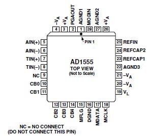
·Automatic Test EquipmentPinout
 Specifications
| Resolution (Bits) |
24bit |
| T-Put Rate |
16kSPS |
| # Chan |
2 |
| Supply V |
Multi(±5, +5 logic) |
| Pwr Diss |
96mW |
| Interface |
Byte,Ser |
| Ain Range |
Bip 2.25V/(PGA Gain) |
| SNR (dB) |
120dB |
| Pkg Type |
LCC |
Analog Inputs
Pins 7, 8, 23, 24, 25, 28 . . . .VA 0.3 V to +VA + 0.3 V
AIN(+), AIN() DC Input Current . . . . . . . . . . . ±100 mA
AIN(+), AIN() 2 s Pulse Input Current . . . . . . . ±1.5 A
Supply Voltages
+VA to VA . . . . . . . . . . . . . . . . . . . . . . 0.3 V to +14 V
+VA to AGND . . . . . . . . . . . . . . . . . . . . . . 0.3 V to +7 V
VA to AGND . . . . . . . . . . . . . . . . . . . . . .7 V to +0.3 V
VL to DGND . . . . . . . . . . . . . . . . . . . . . . . 0.3 V to +7 V
Ground Voltage Differences
DGND, AGND1, AGND2, AGND3 . . . . . . . . . . . . . . ±0.3 V
Digital Inputs . . . . . . . . . . . . . . . . .0.3 V to VL + 0.3 V
Internal Power Dissipation2
AD1555 . . . . . . . . . . . . . . . . . . . . . . . . . . . . . . . . 1.8 W
AD1556 . . . . . . . . . . . . . . . . . . . . . . . . . . . . . . . . 1.8 W
Junction Temperature . . . . . . . . . . . . . . . . . . . . 150°C
Storage Temperature . . . . . . . . . . 65°C to +150°C
Lead Temperature Range
(Soldering 10 sec) . . . . . . . . . . . . . . . . . . . . . . 300°C
NOTES
1 Stresses above those listed under Absolute Maximum Ratings may cause permanent damage to the device. This is a stress rating only; functional operation of the device at these or any other conditions above those indicated in the operational section of this specification is not implied. Exposure to absolute maximum rating conditions for extended periods may affect device reliability.
2 Specification is for device in free air:
28-lead PLCC: JA = 36°C/W, JC = 20°C/W
44-lead MQFP: JA = 36°C/W, JC = 14°C/W
DescriptionThe AD1555 is a complete sigma-delta modulator, combined with a programmable gain amplifier intended for low frequency,high dynamic range measurement applications. The AD1555 outputs a ones-density bitstream proportional to the analog input. When used in conjunction with the AD1556 digital filter/ decimator, a high performance ADC is realized.
The continuous-time analog modulator input architecture avoids the need for an external antialias filter. The programmable gain front end simplifies system design, extends the dynamic range,and reduces the system board area. Low operating power and standby modes makes the AD1555 ideal for remote battery-powered data acquisition systems.
The AD1555 is fabricated on Analog Devices' BiCMOS process that has high performance bipolar devices along with CMOS transistors. The AD1555 and AD1556 are packaged, respectively,in 28-lead PLCC and 44-lead MQFP packages and are specified from 55°C to +85°C (AD1556 and AD1555 B Grade) and from 0°C to 85°C (AD1555 A Grade).

 AD1555 Data Sheet