Features: `256-position, 4-channel
`End-to-end resistance 20 k, 50 k, 200 k
`Pin selectable SPI® or I2C® compatible interface
`Power-on preset to midscale
`Two package address decode pins AD0 and AD1
`Rheostat mode temperature coefficient 30 ppm/°C
`Voltage divider temperature coefficient 5 ppm/°C
`Wide operating temperature range 40°C to +125°C
`5 V to 15 V single supply; ±5 V dual supplyApplication·Mechanical potentiometer replacement
·Optical network adjustment
·Instrumentation: gain, offset adjustment
·Stereo channel audio level control
·Automotive electronics adjustment
·Programmable power supply
·Programmable filters, delays, time constants
·Line impedance matching
·Low resolution DAC/trimmer replacement
·Base station power amp biasing
·Sensor calibrationPinout Specifications
VDD to GND....................0.3 V to +16.5 V
VSS to GND............................0 V to +7.5 V
VDD to VSS.....................................+16.5 V
VL to GND........................0.3 V to +6.5 V
VA, VB, VW to GND....................VSS to VDD
Terminal Current, Ax-Bx, Ax-Wx, Bx-Wx
Pulsed1...................................±20 mA
Continuous....................................±3 mA
Digital Inputs and Output Voltage to GND...0 V to +7 V
Operating Temperature Range........40°C to +85°C
Maximum Junction Temperature (TJ MAX)............150°C
Storage Temperature......................65°C to +150°C
Lead Temperature (Soldering, 10 sec)................300°C
Vapor Phase (60 sec)..........................................215°C
Infrared (15 sec).................................................220°C
Thermal Resistance2 JA
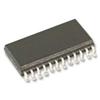
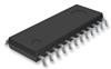
TSSOP-24.......................................................143°C/W
1 Maximum terminal current is bounded by the maximum current handling of the switches, maximum power dissipation of the package, and maximum applied voltage across any two of the A, B, and W terminals at a given resistance.
2 Package power dissipation: (TJMAX TA)/JA.
Stresses above those listed under Absolute Maximum Ratings may cause permanent damage to the device. This is a stress rating only; functional operation of the device at these or any other conditions above those indicated in the operational section of this specification is not implied. Exposure to absolute maximum rating conditions for extended periods may affect device reliability.
| # Channels |
4 |
| # Positions |
256 |
| Memory Type |
Volatile |
| Interface |
I2C,SPI |
| Resistor Values (kOhms) |
20, 50, 200 |
| Bipolar Voltage Range (V) |
±5V |
| Voltage Range (V) |
+15V |
| Supply Current |
1A |
| Temp. Range -40 °C to.. |
125Deg |
| Absolute Tempco (ppm/°C) |
30ppm/C |
| Package |
TSSOP |
DescriptionThe AD5263 is the industry's first quad-channel, 256-position, digital potentiometer1 with a selectable digital interface. This device performs the same electronic adjustment function as mechanical potentiometers or variable resistors, with enhanced resolution, solid-state reliability, and superior low temperature coefficient performance.
Each channel of the AD5263 offers a completely programmable value of resistance between the A terminal and the wiper, or between the B terminal and the wiper. The fixed A-to-B terminal resistance of 20 k, 50 k, or 200 k has a nominal temperature coefficient of ±30 ppm/°C and a ±1% channel-to-channel matching tolerance. Another key feature of this part is the ability to operate from +4.5 V to +15 V, or at ±5 V.
Wiper position programming presets to midscale upon power-on. Once powered, the VR wiper position is programmed by either the 3-wire SPI or 2-wire I2C compatible interface. In the I2C mode, additional programmable logic outputs enable users to drive digital loads, logic gates, and analog switches in their systems.
The AD5263 is available in a narrow body TSSOP-24. All parts are guaranteed to operate over the automotive temperature range of 40°C to +125°C.
For single- or dual-channel applications, refer to the AD5260/AD5280 or AD5262/AD5282.

 AD5263 Data Sheet