AD5311

Features: AD5301: Buffered Voltage Output 8-Bit DACAD5311: Buffered Voltage Output 10-Bit DACAD5321: Buffered Voltage Output 12-Bit DAC6-Lead SOT-23 and 8-Lead mSOIC PackagesMicropower Operation: 120 mA @ 3 V2-Wire (I2C® Compatible) Serial InterfaceData Readback Capability+2.5 V to +5.5 V Powe...

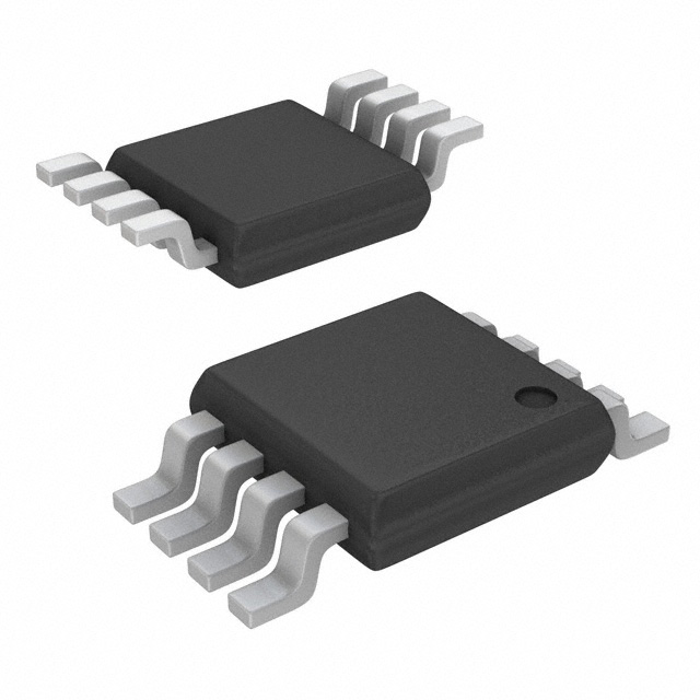
product image

AD5311 Picture
SeekIC No. : 004269061 Detail

AD5311: Features: AD5301: Buffered Voltage Output 8-Bit DACAD5311: Buffered Voltage Output 10-Bit DACAD5321: Buffered Voltage Output 12-Bit DAC6-Lead SOT-23 and 8-Lead mSOIC PackagesMicropower Operation: 12...

floor Price/Ceiling Price

Part Number:
AD5311
Supply Ability:
5000

Price Break

  • Qty
  • 1~5000
  • Unit Price
  • Negotiable
  • Processing time
  • 15 Days
Total Cost: $ 0.00

SeekIC Buyer Protection PLUS - newly updated for 2013!

  • Escrow Protection.
  • Guaranteed refunds.
  • Secure payments.
  • Learn more >>

Month Sales

268 Transactions

Rating

evaluate  (4.8 stars)

Upload time: 2025/12/4

Payment Methods

All payment methods are secure and covered by SeekIC Buyer Protection PLUS.

Notice: When you place an order, your payment is made to SeekIC and not to your seller. SeekIC only pays the seller after confirming you have received your order. We will also never share your payment details with your seller.
Product Details

Description


Features:

AD5301: Buffered Voltage Output 8-Bit DAC
AD5311: Buffered Voltage Output 10-Bit DAC
AD5321: Buffered Voltage Output 12-Bit DAC
6-Lead SOT-23 and 8-Lead mSOIC PackagesMicropower Operation: 120 mA @ 3 V2-Wire (I2C® Compatible) Serial InterfaceData Readback Capability+2.5 V to +5.5 V Power SupplyGuaranteed Monotonic By Design Over All CodesPower-Down to 50 nA @ 3 VReference Derived from Power SupplyPower-On-Reset to Zero VoltsOn-Chip Rail-to-Rail Output Buffer AmplifierThree Power-Down Functions


Application

Portable Battery Powered Instruments
Digital Gain and Offset Adjustment
Programmable Voltage and Current Sources
Programmable Attenuators


Pinout

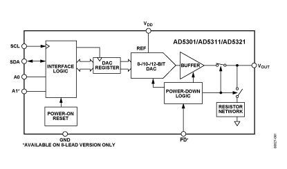
  Connection Diagram

AD5311 Diagram


Specifications

VDD to GND . . . . . . . . . . . . . . . . . . . . . . . . . . . 0.3 V to +7 V
SCL, SDA to GND . . . . . . . . . . . . . . . . 0.3 V to VDD + 0.3 V
PD, A1, A0 to GND . . . . . . . . . . . . . . . 0.3 V to VDD + 0.3 V
VOUT to GND . . . . . . . . . . . . . . . . . . . . 0.3 V to VDD + 0.3 V
Operating Temperature Range
Industrial (B Version) . . . . . . . . . . . . . . . . 40 to +105
Storage Temperature Range . . . . . . . . . . . . . 65 to +150
Junction Temperature (TJ max) . . . . . . . . . . . . . . . . . . .+150
SOT-23 Package
Power Dissipation . . . . . . . . . . . . . . . . . . . (TJ max TA)/qJA
qJA Thermal Impedance . . . . . . . . . . . . . . . . . . . . 229.6/W
mSOIC Package
Power Dissipation . . . . . . . . . . . . . . . . . . . (TJ max TA)/qJA
qJA Thermal Impedance . . . . . . . . . . . . . . . . . . . . . 206/W
Lead Temperature, Soldering
Vapor Phase (60 sec) . . . . . . . . . . . . . . . . . . . . . . . . +215
Infrared (15 sec) . . . . . . . . . . . . . . . . . . . . . . . . . . . . +220


Resolution (Bits) 10bit
DAC Update Rate 143kSPS
DAC Settling Time 7s
# DAC Outputs 1
DAC Type Voltage Out
DAC Input Format I2C/Ser 2-wire,Ser
Output FSR (Uni Vdd)
Ref Int/Ext Ext
Supply Vnom Single(+2.5),Single(+2.7),Single(+3),Single(+3.3),Single(+5)
Pwr Diss 1.4mW
Package SOP,SOT


Description

The AD5301/AD5311/AD5321 are single 8-, 10- and 12-bitbuffered voltage-output DACs that operate from a single +2.5 Vto +5.5 V supply consuming 120 mA at 3 V. The on-chip outputamplifier allows rail-to-rail output swing with a slew rate of0.7 V/ms. It uses a 2-wire (I2C compatible) serial interface thatoperates at clock rates up to 400 kHz. Multiple devices canshare the same bus.


The reference for the DAC AD5301/AD5311/AD5321 is derived from the power supplyinputs and thus gives the widest dynamic output range. Theseparts incorporate a power-on-reset circuit, which ensures thatthe DAC output powers-up to zero volts and remains there untila validwrite takes place. The parts contain a power-down featurewhich reduces the current consumption of the device to 50 nAat 3 V and provides software-selectable output loads while inpower-down mode.


The low power consumption in normal operation make theseDACs AD5301/AD5311/AD5321 ideally suited to portable battery-operated equipment.The power consumption is 0.75 mW at 5 V, 0.36 mW at 3 Vreducing to 1 mW in all power-down modes.


Customers Who Bought This Item Also Bought

Margin,quality,low-cost products with low minimum orders. Secure your online payments with SeekIC Buyer Protection.
Circuit Protection
Motors, Solenoids, Driver Boards/Modules
Power Supplies - External/Internal (Off-Board)
Resistors
View more