Features: AD5308: 8 Buffered 8-Bit DACs in 16-Lead TSSOPA Version: ±1 LSB INL, B Version: ±0.75 LSB INLAD5318: 8 Buffered 10-Bit DACs in16-Lead TSSOPA Version: ±4 LSB INL, B Version: ±3 LSB INLAD5328: 8 Buffered 12-Bit DACs in 16-Lead TSSOPA Version: ±16 LSB INL, B Version: ±12 LSB INLLow Power Operation: 0.7 mA @ 3 VGuaranteed Monotonic by Design over All CodesPower-Down to 120 nA @ 3 V, 400 nA @ 5 VDouble-Buffered InputLogicBuffered/Unbuffered/VDD Reference Input OptionsOutput Range: 0 V to VREF or 0 V to 2 VREFPower-On Reset to 0 VProgrammabilityIndividual Channel Power-DownSimultaneous Update of Outputs (LDAC)Low Power, SPI®, QSPI™, MICROWIRE™, and DSPCompatible 3-Wire Serial InterfaceOn-Chip Rail-to-Rail Output Buffer AmplifiersTemperature Range 40�C to +105 ApplicationPortable Battery-Powered InstrumentsDigital Gain and Offset AdjustmentProgrammable Voltage and Current SourcesOptical NetworkingAutomatic Test EquipmentPinout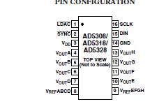 Specifications
| Resolution (Bits) |
10bit |
| DAC Update Rate |
167kSPS |
| DAC Settling Time |
6s |
| # DAC Outputs |
8 |
| DAC Type |
Voltage Out |
| DAC Input Format |
Ser,SPI |
| Output FSR |
(Uni 2Vref),(Uni Vref) |
| Ref Int/Ext |
Ext |
| Supply Vnom |
Single(+2.5),Single(+2.7),Single(+3),Single(+3.3),Single(+5) |
| Pwr Diss |
4.5mW |
| Package |
SOP |
(TA = 25°C, unless otherwise noted.)
VDD to GND . . . . . . . . . . . . . . . . . . . . . . . . . . . 0.3 V to +7 V
Digital Input Voltage to GND . . . . . . . . .0.3 V to VDD + 0.3 V
Reference Input Voltage to GND . . . . . .0.3 V to VDD + 0.3 V
VOUTAVOUTD to GND . . . . . . . . . . .. . 0.3 V to VDD + 0.3 V
Operating Temperature Range
Industrial (A, B Version) . . . . . . . . . . . . . . . 40 to +105
Storage Temperature Range . . . . . . . . . . . . 65 to +150
Junction Temperature (TJ MAX) . . . . . . . . . . . . . . . . . . .150DescriptionThe AD5308/AD5318/AD5328 are octal 8-, 10-, and 12-bit buffered voltage output DACs in a 16-lead TSSOP. They operate from a single 2.5 V to 5.5 V supply, consuming 0.7 mA typical at 3 V. Their on-chip
The AD5308/AD5318/AD5328 are octal 8-, 10-, and 12-bitbuffered voltage output DACs in a 16-lead TSSOP. They operatefrom a single 2.5 V to 5.5 V supply, consuming 0.7 mA typ at 3 V.Their on-chip output amplifiers allow the outputs to swingrail-to-rail with a slew rate of 0.7 V/s. The AD5308/AD5318/AD5328 use a versatile 3-wire serial interface that operates atclock rates up to 30 MHz and is compatible with standardSPI, QSPI, MICROWIRE, and DSP interface standards.
The references for the eight DACs AD5308/AD5318/AD5328 are derived from two referencepins (one per DAC quad). These reference inputs can beconfigured as buffered, unbuffered, or VDD inputs. The partsincorporate a power-on reset circuit, which ensures that the DACoutputs power up to 0 V and remain there until a valid write tothe device takes place. The outputs of all DACs may be updatedsimultaneously using the asynchronousLDAC input. The partscontain a power-down feature that reduces the current consumptionof the devices to 400 nA at 5 V (120 nA at 3 V). The eightchannels of the DAC may be powered down individually.
All three parts AD5308/AD5318/AD5328 are offered in the same pinout, which allowsusers to select the resolution appropriate for their applicationwithout redesigning their circuit board.

 AD5318 Data Sheet