Features: `2 V to +6 V Output Range
`2.5 Output Resistance
`2.5 ns Tr/Tf for a 3 V Step
`300 MHz Toggle Rate
`Can Drive 25 Lines and Lower
`Peak Dynamic Current Capability of 400 mA
`Inhibit Leakage <1 A
`On-Chip Temperature SensorApplicationAutomatic Test Equipment
Semiconductor Test Systems
Board Test Systems
Instrumentation and Characterization EquipmentPinout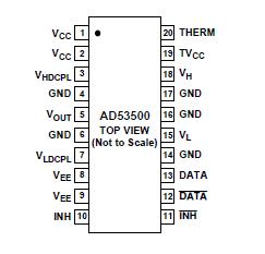 Specifications
Power Supply Voltage
+VS to GND . . . . . . . . . . . . . . . . . . . . . . . . . . . . . . .+11 V
VS to GND . . . . . . . . . . . . . . . . . . . . . . . . . . . . . . .7 V
+VS to VS . . . . . . . . . . . . . . . . . . . . . . . . . . . . . . .+18 V
Inputs
DATA, DATA, INH,INH . . . . . . . . . . . . . . . . . . +5 V, 3 V
DATA to DATA, INH toINH . . . . . . . . . . . . . . . . . . . . ±3 V
VH, VL to GND . . . . . . . . . . . . . . . . . . . . . . . . . +7 V, 3 V
VH to VL . . . . . . . . . . . . . . . . . . . . . . . . . . . . . . +10 V, 0 V
Outputs
VOUT Short Circuit Duration to Ground . . . . . . Indefinite2
VOUT Range in Inhibit Mode . . . . . . . . . . . . . See Figure 1
VHDCPL . . . . . . . .Do Not Connect Except for Cap to VCC3
VLDCPL . . . . . . . . Do Not Connect Except for Cap to VEE3
THERM . . . . . . . . . . . . . . . . . . . . . . . . . . . . . . . . +VS, 0 V
Environmental
Operating Temperature (Junction) . . . . . . . . . . . +175°C
Storage Temperature . . . . . . . . . . . . .65°C to +150°C
Lead Temperature (Soldering, 10 sec)4 . . . . . . . .+260°C
NOTES
1 Stresses above those listed under Absolute Maximum Ratings may cause permanent damage to the device. This is a stress rating only; functional operation of the device at these or any other conditions above those indicated in the operational sections of this specification is not implied. Absolute maximum limits apply individually, not in combination. Exposure to absolute maximum rating conditions for extended periods may affect device reliability.
2 Output short circuit protection is guaranteed as long as proper heat sinking is employed to ensure compliance with the operating temperature limits.
3 The VHDCPL and VLDCPL capacitors may be replaced by a low value resistor for higher dc-current drive capability.
4To ensure lead coplanarity (±0.002 inches) and solderability, handling with bare hands should be avoided and the device should be stored in environments at 24°C ± 5°C (75°F ± 10°F) with relative humidity not to exceed 65%.
| Package |
20-Lead PSOP |
| Vmax |
6 |
| Vmin |
-2 |
| Watts Per Channel (W) |
1.4W |
| Channels |
1 |
| Configuration |
D |
DescriptionThe AD53500 is a complete high speed driver designed for use in digital or mixed signal test systems where high speed and high output drive capabilities are needed. Combining a high speed monolithic process and a unique surface mount package, this product attains superb electrical performance while preserving optimum packing densities and long-term reliability thanks to an ultrasmall 20-lead, PSOP package with built-in heat sink.
High and low reference levels can be set within a 2 V to +6 V range with low offset voltage and high gain accuracy. A 2.5 output resistance allows use of an external backmatch resistor AD53500 for application to 50 W, 25 or other complex impedance load requirements. Without a backmatch resistor it is also capable of driving highly capacitive loads, typically achieving a rise/fall time of less than 10 ns with a 1000 pF capacitance. To test I/O devices, the pin driver can be switched into a high impedance state (Inhibit Mode), electrically removing the driver from the path. The pin driver leakage current in inhibit is typically less than 1 mA and output capacitance is typically less than 18 pF.
Transitions AD53500 from HI/LO or to inhibit are controlled through the data and inhibit inputs. The input circuitry utilizes high-speed differential inputs with a common-mode range of 2 V to +5 V.This allows for direct interface to the precision of differential ECL timing or the simplicity of stimulating the pin driver from a single-ended CMOS or TTL logic source or any combination over the common-mode range. The analog logic HI/LO inputs are equally easy to interface, typically requiring 50 mA of bias current.

 AD53500 Data Sheet