Features: `500 MHz Driver Operation (1 Gb/s)
`Driver Inhibit Function
`100 ps Edge Matching
`Guaranteed Industry Specifications
20 Output Impedance
5 V/ns Slew Rate
Variable Output Voltages for ECL, TTL, and CMOS
`High-Speed Differential Inputs for Maximum Flexibility Ultrasmall 100-Lead LQFP Package with Built-In
Heat Sink
Application·Automatic Test Equipment
Semiconductor Test Systems
Board Test Systems
·Instrumentation and Characterization EquipmentPinout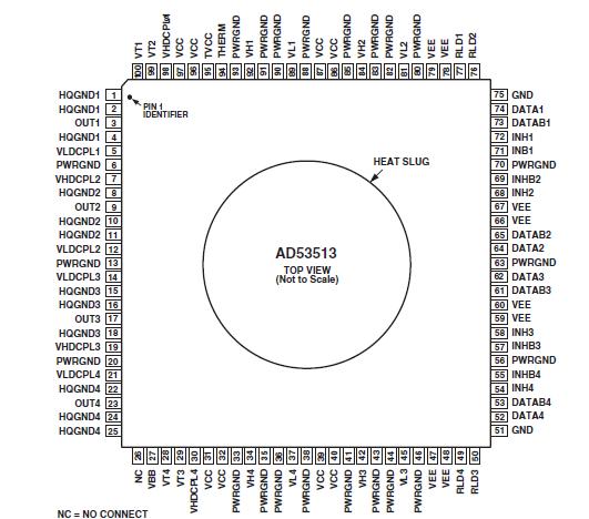 Specifications
Power Supply Voltage
+VS to GND . . . . . . . . . . . . . . . . . . . . . . . . . . . . . . . 11 V
VS to GND . . . . . . . . . . . . . . . . . . . . . . . .. . . . . . 7 V
+VS to VS . . . . . . . . . . . . . . . . . . . . . . . . . . . . . . . 18 V
Inputs
DATA, DATA, INH, INH, RLD, VBB . . . . . . . . . +5 V, 3 V
DATA to DATA, INH to INH, RLD, VBB . . . . . . . . . . . ±3 V
VH, VL, VT to GND . . . . . . . . . . . . . . . . . . . . . +7 V, 2 V
VH to VL (VH VT) and (VT VL) . . . . . . . . . . . . . ±9 V
Outputs
VOUT Short Circuit Duration . . . . . . . .. . . . . . Indefinite2
VOUT Range in Inhibit Mode
VHDCPL . . . . Do Not Connect Except for Capacitor to VCC
VLDCPL . . . . Do Not Connect Except for Capacitor to VEE
THERM . . . . . . . . . . . . . . . . . . . . . . . . . . . . . . . 11 V, 0 V
Environmental
Operating Temperature (Junction) . . . . . . . . . . . 175°C
Storage Temperature . . . . . . . . . . 65°C to +150°C
Lead Temperature (Soldering, 10 sec)3 . . . . . . . 260°C
NOTE
1Stresses above those listed under Absolute Maximum Ratings may cause permanent damage to the device. This is a stress rating only; functional operation of the device at these or any other conditions above those indicated in the operational sections of this specification is not implied. Absolute maximum limits apply individually, not in combination. Exposure to absolute maximum rating conditions for extended periods may affect device reliability.
2Output short circuit protection is guaranteed as long as proper heat sinking is employed to ensure compliance with the operating temperature limits.
3To ensure lead coplanarity (± 0.002 inches) and solderability, handling with bare hands should be avoided and the device should be stored in environments at 24 °C ±5°C (75°F ±10°F) with relative humidity not to exceed 65%.
DescriptionThe AD53513 is a quad high-speed pin driver designed for use in digital or mixed-signal test systems. Combining a high-speed monolithic process with a convenient surface-mount package, this product attains superb electrical performance while preserving optimum packaging densities and long-term reliability in a 100-lead, LQFP package with built-in heat sink.
Featuring unity gain programmable output levels of 2.5 V to +5.5 V, with output swing capability of less than 200 mV to 8 V, the AD53513 is designed to stimulate ECL, TTL, and CMOS logic families, as well as high-speed memory. The 1.0 Gb/s data rate capacity and matched output impedance allow for real-time stimulation of these digital logic families. To test I/O devices, the pin driver can be switched into a high impedance state (Inhibit Mode), electrically removing the driver from the path. The pin driver leakage current in inhibit is typically 100 nA and output charge transfer entering inhibit is typically less than 20 pC.
The AD53513 transition from HI/LO or to inhibit is controlled through the data and inhibit inputs. The input circuitry uses high-speed differential inputs with a common-mode range of ±2 V. This allows for direct interface to precision differential ECL timing. The analog logic HI/LO inputs are equally easy to interface. Typically requiring 10 A of bias current, the AD53513 can be directly coupled to the output of a digitalto- analog converter.
Each channel of the AD53513 has a Mode Select Pin RLD, which is a single-sided logic input. The logic threshold is set by the VBB input which is common to all four channels. The RLD Mode Select controls whether inhibit puts the driver in High-Z or VTERM mode. (Refer to Table I.) All of the digital logic inputs (DATA, DATAB, INH, INHB, RLD, VBB), must share a common set of logic levels. The VBB threshold should be set to the midrange of the logic levels. For example, if ECL levels of 0.8 V to 1.8 V are used, VBB should be set to 1.3 V.
The AD53513 is available in a 100-lead, LQFP package with a built-in heat sink and is specified to operate over the ambient commercial temperature range of 25°C to +85°C.

 AD53513 Data Sheet