Features: `1000 MHz Toggle Rate
`Driver/Comparator/Active Load and Dynamic Clamp Included
`Inhibit Mode Function
`100-Lead LQFP Package with Built-In Heat Sink
48 Output Resistance
800 ps Tr/Tf for a 3 V Step
`Comparator
1.1 ns Propagation Delay at 3 V
`Load
±40 mA Voltage Programmable Current Range
50 ns Settling Time to 15 mVApplicationAutomatic Test Equipment
Semiconductor Test Systems
Board Test Systems
Instrumentation and Characterization EquipmentPinout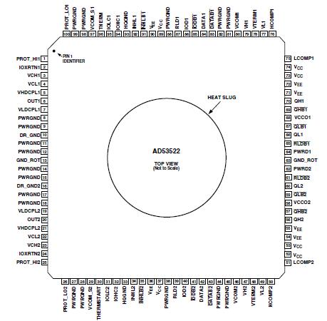 Specifications
POWER SUPPLY VOLTAGE
VCC to GND . . . . . . . . . . . . . . . . . . . . . . . . . . . . . . . 11.3 V
VEE to GND . . . . . . . . . . . . . . . . . . . . . . . . . . . . . . . . 7 V
VCC to VEE . . . . . . . . . . . . . . . . . . . . . . . . . . . . . . . . . 18 V
VCCO to GND . . . . . . . . . . . . . . . . . . . . . . . . . . . . . . .5.5 V
PWRGND, DRGND, GND_ROT, or HQGND . . . . . . . . .±0.4 V
OUTPUTS
VOUT Short Circuit Duration . . . . . . . . . . . . . . .. Indefinite2
VOUT, Inhibit Mode . . . . . . . . . . . . . . . . . . . . .+8.5 V, 2 V
VOUT, Inhibit Mode . . . . . VL 5.5 V < VOUT < VH + 5.5 V
VHDCPL . . . . . . . . . Do Not Connect Except for Cap to VCC
VLDCPL . . . . . . . . . . Do Not Connect Except for Cap to VEE
QH, QHb, QL, QLB Maximum IOUT:
Continuous . . . . . . . . . . . . . . . . . . . . . . . . . . . . . . . . 50 mA
Surge . . . . . . . . . . . . . . . . . . . . . . . . . . . . . . . . . . . .100 mA
THERM . . . . . . . . . . . . . . . . . . . . . . . . . . . . . . . . . 11 V, 0 V
Driver output capacitance, maximum . . . . . . . . . . . . . . 10 pF
INPUTS
DATA, DATAb, IOD, IODb, RLD, RLDB . . .(VCCO + 1.5 V,VCCO 4.5 V)
INHL, INHLb, CMPD . . . . . . . . . . . . . . . . . . . 0.4 V to +5.5 V
PWRD . . . . . . . . . . . . . . . . . . . . . . . . . . . . . 0.4 V to +4.5 V
DATA to DATAb, IOD to IODb, RLD to RLDB . . . . . . . . . . .±3 V
INHL to INHLb . . . . . . . . . . . . . . . . . . . . . . . . . . . . . . . . ±6 V
VH, VL, VTERM to GND (Rseries < 500 ) . . . . .+7.5 V, 1.1 V
VH to VL . . . . . . . . . . . . . . . . . . . . . . . . . . . . . . . +8 V, 3.5 V
(VH VTERM) and (VTERM VL) . . . . . . . . . . . . . . . . . . ±8 V
Reflection Clamps High/Low . . . . . . . . . . . . . . . . +8.5 V, 2 V
Protection Clamp Breakdown Voltage . . . . . . . . . . . . . . . 12 V
Protection Clamps Current . . . . . . . . . . . . . . . . . . . . . ±5 mA
VOUT to HCOMP or LCOMP . . . . . . . . . . . . . . . . . . . . . .±7.8 V
ENVIRONMENTAL
Operating Temperature (Junction) . . . . . . . . . . . . . . . . 175°C
Storage Temperature . . . . . . . . . . . . . . . . 65°C to +150°C
Lead Temperature (Soldering, 10 sec)3 . . . . . . . . . . . . 260°C
NOTES
1 Stresses above those listed under Absolute Maximum Ratings may cause permanent damage to the device. This is a stress rating only; functional operation of the device at these or any other conditions above those indicated in the operational sections of this specification is not implied. Absolute maximum limits apply individually, not in combination. Exposure to absolute maximum rating conditions for extended periods may affect device reliability.
2 Output short circuit protection is guaranteed as long as proper heat sinking is employed to ensure compliance with the operating temperature limits.
3 To ensure lead coplanarity (± 0.002 inches) and solderability, handling with bare hands should be avoided and the device should be stored in environments at 24 °C ± 5°C (75°F ± 10°F) with relative humidity not to exceed 65%.
DescriptionThe AD53522 is a complete, high-speed, single-chip solution that performs the pin electronics functions of driver, comparator,and active load (DCL) for ATE applications. In addition, the driver contains a dynamic clamp function and the active load contains an integrated Schottky diode bridge.
The driver AD53522 is a proprietary design that features three active states:Data High Mode, Data Low Mode, and Term Mode, as well as an Inhibit State. In conjunction with the integrated dynamic clamp this facilitates the implementation of a high-speed active termination. The output voltage range is 0.5 V to +6.5 V to accommodate a wide variety of test devices.
The dual comparator AD53522, with an input range equal to the driver output range, features PECL compatible outputs. Signal tracking capability is in the range of 3 V/ns.
The active load can be set for up to 40 mA load current. IOH,IOL, and the buffered VCOM are independently adjustable.On-board Schottky diodes provide high-speed switching and low capacitance.
Also included on the chip is an on-board temperature sensor that gives an indication of the silicon surface temperature of the DCL. This information can be used to measure JC and JA or flag an alarm if proper cooling is lost. Output from the sensor is a current sink that is proportional to absolute temperature.The gain is trimmed to a nominal value of 1.0 A/k. As an example, the output current can be sensed by using a 10 k resistor connected from 10 V to the THERM (IOUT) pin. A voltage drop across the resistor will be developed that equals:10 k * 1 A/k = 10 V/k = 2.98 V at room temperature.

 AD53522 Data Sheet