Features: ·AD5390: 16-channel, 14-bit voltage output DAC
·AD5391: 16-channel, 12-bit voltage output DAC
·AD5392: 8-channel, 14-bit voltage output DAC
·Guaranteed monotonic
·INL: ±1 LSB max (AD5391)
±3 LSB max (AD5390-5/AD5392-5)
±4 LSB max (AD5390-3/AD5392-3)
·On-chip 1.25 V/2.5 V, 10 ppm/°C reference
·Temperature range: −40°C to +85°C
·Rail-to-rail output amplifier
·Power-down mode
·Package types:
64-lead LFCSP (9 mm × 9 mm)
52-lead LQFP (10 mm × 10 mm)
·User interfaces:Serial SPI®-, QSPI™-, MICROWIRE™-, and DSP-compatible (featuring data readback)
·I2C®-compatible interfaceApplication·Instrumentation and industrial control
·Power amplifier control
·Level setting (ATE)
·Control systems
·Microelectromechanical systems (MEMs)
·Variable optical attenuators (VOAs)
·Optical transceivers (MSA 300, XFP)Pinout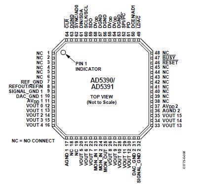 Specifications
| Resolution (Bits) |
14bit |
| DAC Update Rate |
125kSPS |
| DAC Settling Time |
8s |
| # DAC Outputs |
16 |
| DAC Type |
Voltage Out |
| DAC Input Format |
I2C/Ser 2-wire,Ser,SPI |
| Output FSR |
(Uni 2.5V),(Uni 2Vref),(Uni 5V),User Def. Range/Offset |
| Ref Int/Ext |
Int/Ext |
| Supply Vnom |
Single(+3),Single(+3.3),Single(+5) |
| Package |
CSP,QFP |
AVDD to AGND.................................−0.3 V to +7 V
DVDD to DGND.................................−0.3 V to +7 V
Digital Inputs to DGND.......−0.3 V to DVDD + 0.3 V
Digital Outputs to DGND....−0.3 V to DVDD + 0.3 V
VREF to AGND.................................−0.3 V to +7 V
REFOUT to AGND.............................−0.3 V to +7 V
AGND to DGND.............................−0.3 V to +0.3 V
VOUTX to AGND. ................−0.3 V to AVDD + 0.3 V
Operating Temperature Range
Commercial (B Version).........−40°C to +85°C
Storage Temperature Range....−65°C to +150°C
Junction Temperature (TJ max)...................150°C
64-Lead LFCSP Package, JA.................22°C/W
52-lLad LQFP Package, JA....................38°C/W
Reflow Soldering Peak Temperature............230°C
Stresses above absolute maximum ratings may cause permanent damage to the device. This is a stress rating only; functional operation of the device at these or any other conditions above those listed in the operational sections of this specification is not implied. Exposure to absolute maximum rating conditions for extended periods may affect device reliability.
DescriptionThe AD5390/AD5391 are complete single-supply, 16-channel, 14-bit and 12-bit DACs, respectively. The AD5392 is a complete single-supply, 8-channel, 14-bit DAC. Devices are available both in 64-lead LFCSP and 52-lead LQFP packages. All channels have an on-chip output amplifier with rail-to-rail operation. All devices include an internal 1.25/2.5 V, 10 ppm/°C reference, an on-chip channel monitor function that multiplexes the analog outputs to a common MON_OUT pin for external monitoring, and an output amplifier boost mode that optimizes the output amplifier slew rate.
The AD5390/AD5391/AD5392 contain a 3-wire serial interface with interface speeds in excess of 30 MHz that are compatible with SPI, QSPI, MICROWIRE, and DSP interface standards and an I2C-compatible interface supporting a 400 kHz data transfer rate.
An input register followed by a DAC register provides double-buffering, allowing DAC outputs to be updated independently or simultaneously using theLDAC input. Each channel has a programmable gain and offset adjust register, letting the user fully calibrate any DAC channel.
Power consumption is typically 0.25 mA per channel.

 AD5390 Data Sheet