AD660

Features: · Complete 16-Bit D/A Function On-Chip Output Amplifier On-Chip Buried Zener Voltage Reference· ±1 LSB Integral Linearity· 15-Bit Monotonic over Temperature· Microprocessor Compatible Serial or Byte Input Double Buffered Latches Fast (40 ns) Write Pulse· Asynchronous Clear (to 0 V) Funct...

product image

AD660 Picture
SeekIC No. : 004269698 Detail

AD660: Features: · Complete 16-Bit D/A Function On-Chip Output Amplifier On-Chip Buried Zener Voltage Reference· ±1 LSB Integral Linearity· 15-Bit Monotonic over Temperature· Microprocessor Compatible Seri...

floor Price/Ceiling Price

Part Number:
AD660
Supply Ability:
5000

Price Break

  • Qty
  • 1~5000
  • Unit Price
  • Negotiable
  • Processing time
  • 15 Days
Total Cost: $ 0.00

SeekIC Buyer Protection PLUS - newly updated for 2013!

  • Escrow Protection.
  • Guaranteed refunds.
  • Secure payments.
  • Learn more >>

Month Sales

268 Transactions

Rating

evaluate  (4.8 stars)

Upload time: 2024/4/26

Payment Methods

All payment methods are secure and covered by SeekIC Buyer Protection PLUS.

Notice: When you place an order, your payment is made to SeekIC and not to your seller. SeekIC only pays the seller after confirming you have received your order. We will also never share your payment details with your seller.
Product Details

Description


Features:

· Complete 16-Bit D/A Function
  On-Chip Output Amplifier
  On-Chip Buried Zener Voltage Reference
· ±1 LSB Integral Linearity
· 15-Bit Monotonic over Temperature
· Microprocessor Compatible
  Serial or Byte Input
  Double Buffered Latches
  Fast (40 ns) Write Pulse
· Asynchronous Clear (to 0 V) Function
· Serial Output Pin Facilitates Daisy Chaining
· Unipolar or Bipolar Output
· Low Glitch: 15 nV-s
· Low THD+N: 0.009%


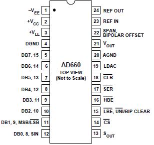
Pinout

  Connection Diagram


Specifications

VCC to AGND . . . . . . . . . . . . . . . . . . . . . ..0.3 V to +17.0 V
VEE to AGND . . . . . . . . . . . . . . . . . . . . . . .+0.3 V to 17.0 V
VLL to DGND . . . . . . . . . . . . . . . . . . . . . . . . . 0.3 V to +7 V
AGND to DGND . . . . . . . . . . . . . . . . . . . . . . . . . . . . .. . ±1 V
Digital Inputs (Pins 5 through 23) to DGND . . . . . .1.0 V to
                                                                                  +7.0 V
REF IN to AGND . . . . . . . . . . . . . . . . . . . . . . . . . . . .±10.5 V
Span/Bipolar Offset to AGND . . . . . . . . . . . . . . . . ..±10.5 V
Ref Out, VOUT . . . . . . ...... Indefinite Short to AGND, DGND,
                                                               VCC, VEE, and VLL
Power Dissipation (Any Package)
To +60°C . . . . . . . . . . . . . . . . . . . . . . . . . . . . . . 1000 mW
Derates above +60°C . . . . . . . . . . . . . . . . . . . 8.7 mW/°C
Storage Temperature . . . . . . . . . . . . . . .65°C to +150°C
Lead Temperature Range
(Soldering 10 sec) . . . . . . . . . . . . . . . . . . . . . . . . . +300°C

*Stresses above those listed under "Absolute Maximum Ratings" may cause permanent damage to the device. This is a stress rating only and functional operation of the device at these or any other conditions above those indicated in the operational section of this specification is not implied. Exposure to absolute maximum rating conditions for extended periods may affect device reliability.


Description

The AD660 DACPORT™ is a complete 16-bit monolithic D/A converter with an on-board voltage reference, double buffered latches and output amplifier. It is manufactured on Analog Devices' BiMOS II process. This process allows the fabrication of low power CMOS logic functions on the same chip as high precision bipolar linear circuitry.

The AD660's architecture ensures 15-bit monotonicity over time and temperature. Integral and differential nonlinearity is maintained at ±0.003% max. The on-chip output amplifier provides a voltage output settling time of 10 ms to within 1/2 LSB for a full-scale step.

The AD660 has an extremely flexible digital interface. Data can be loaded into the AD660 in serial mode or as two 8-bit bytes. This is made possible by two digital input pins which have dual functions. The serial mode input format is pin selectable to be MSB or LSB first. The serial output pin allows the user to daisy chain several AD660s by shifting the data through the input latch into the next DAC thus minimizing the number of control  lines required to SIN, CS and LDAC. The byte mode input format is also flexible in that the high byte or low byte data can be loaded first. The double buffered latch structure eliminates data skew errors and provides for simultaneous updating of DACs in a multi-DAC system.

The AD660 is available in five grades. AN and BN versions are specified from 40°C to +85°C and are packaged in a 24-pin 300 mil plastic DIP. AR and BR versions are also specified from 40°C to +85°C and are packaged in a 24-pin SOIC. The SQ version is packaged in a 24-pin 300 mil cerdip package and is also available compliant to MIL-STD-883. Refer to the AD660/883B data sheet for specifications and test conditions.


Customers Who Bought This Item Also Bought

Margin,quality,low-cost products with low minimum orders. Secure your online payments with SeekIC Buyer Protection.
Circuit Protection
Batteries, Chargers, Holders
Cables, Wires - Management
Computers, Office - Components, Accessories
LED Products
View more