Features: ·12-bit plus sign SAR ADC
·True bipolar input ranges
·Software-selectable input ranges
±10 V, ±5 V, ±2.5 V, 0 V to 10 V
·1 MSPS throughput rate
·Eight analog input channels with channel sequencer
·Single-ended, true differential, and pseudo differential analog input capability
·High analog input impedance
·Low power: 21 mW
·Temperature indicator
·Full power signal bandwidth: 22 MHz
·Internal 2.5 V reference
·High speed serial interface
·Power-down modes
·20-lead TSSOP package
·iCMOS™ process technologyPinout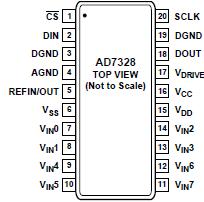
 Specifications
VDD to AGND, DGND ...................................−0.3 V to +16.5 V
VSS to AGND, DGND.................................... +0.3 V to −16.5 V
VDD to Vcc..............................................Vcc − 0.3 V to 16.5 V
VCC to AGND, DGND.........................................−0.3 V to +7 V
VDRIVE to AGND, DGND....................................−0.3 V to +7 V
AGND to DGND..............................................−0.3 V to +0.3 V
Analog Input Voltage to AGND1....VSS − 0.3 V to VDD + 0.3 V
Digital Input Voltage to DGND.........................−0.3 V to +7 V
Digital Output Voltage to GND.........−0.3 V to VDRIVE + 0.3 V
REFIN to AGND.....................................−0.3 V to VCC + 0.3 V
Input Current to any Pin Except Supplies2...............±10 mA
Operating Temperature Range..................−40°C to +85°C
Storage Temperature Range...................−65°C to +150°C
Junction Temperature.................................................150°C
TSSOP Package
JA Thermal Impedance.........................................143°C/W
JC Thermal Impedance...........................................45°C/W
Pb-free Temperature, Soldering
Reflow....................................................................260(0)°C
ESD..............................................................................2.5 kV
1 If the analog inputs are driven from alternative VDD and VSS supply circuitry, Schottky diodes should be placed in series with the AD7328's VDD and VSS supplies.
2 Transient currents of up to 100 mA do not cause SCR latch-up.
Stresses above those listed under Absolute Maximum Ratings may cause permanent damage to the device. This is a stress rating only; functional operation of the device at these or any other conditions above those indicated in the operational section of this specification is not implied. Exposure to absolute maximum rating conditions for extended periods may affect device reliability
| Resolution (Bits) |
13bit |
| T-Put Rate |
1MSPS |
| # Chan |
8 |
| Supply V |
Multi(±12, +5),Multi(±15, +3) ,Multi(±15, +3.3),Multi(±15, +5) |
| Pwr Diss (max) |
29mW |
| Interface |
Ser,SPI |
| Ain Range |
Bip (Vref),Bip (Vref) x 2,Bip (Vref) x 4,Bip 10V,Bip 2.5V,Bip 5.0V,Uni (Vref) x 4,Uni 10V |
| SNR (dB) |
76dB |
| Pkg Type |
SOP |
DescriptionThe AD73281 is an 8-channel, 12-bit plus sign successive approximation ADC designed on the iCMOS (industrial CMOS) process. iCMOS is a process combining high voltage CMOS and low voltage CMOS. It enables the development of a wide range of high performance analog ICs capable of 33 V operation in a footprint that no previous generation of high voltage parts could achieve. Unlike analog ICs using conven-tional CMOS processes, iCMOS components can accept bipolar input signals while providing increased performance, dramatically reducing power consumption, and having a reduced package size.
The AD7328 can accept true bipolar analog input signals. The AD7328 has four software-selectable input ranges, ±10 V, ±5 V, ±2.5 V, and 0 V to 10 V. Each analog input channel can be indepen-dently programmed to one of the four nput ranges. The analog input channels on the AD7328 can be programmed to be single-ended, true differential, or pseudo differential.
The ADC contains a 2.5 V internal reference. The AD7328 also allows for external reference operation. If a 3 V reference is applied to the REFIN/OUT pin, the AD7328 can accept a true bipolar ±12 V analog input. Minimum ±12 V VDD and VSS supplies are required for the ±12 V input range. The ADC has a high speed serial interface that can operate at throughput rates up to 1 MSPS.

 AD7328 Data Sheet