Features: Fast Throughput Rate: 1MSPS
Specified for VDD of 3 V and 5 V
Low Power at max Throughput Rate:
3 mW typ at 833kSPS with 3 V Supplies
8 mW typ at 1MSPS with 5 V Supplies
Fully Differential Analog Input
Wide Input Bandwidth:
70dB SINAD at 300kHz Input Frequency
Flexible Power/Serial Clock Speed Management
No Pipeline Delays
High Speed Serial Interface - SPITM/QSPITM/
MicroWireTM/ DSP Compatible
Powerdown Mode: 1A max
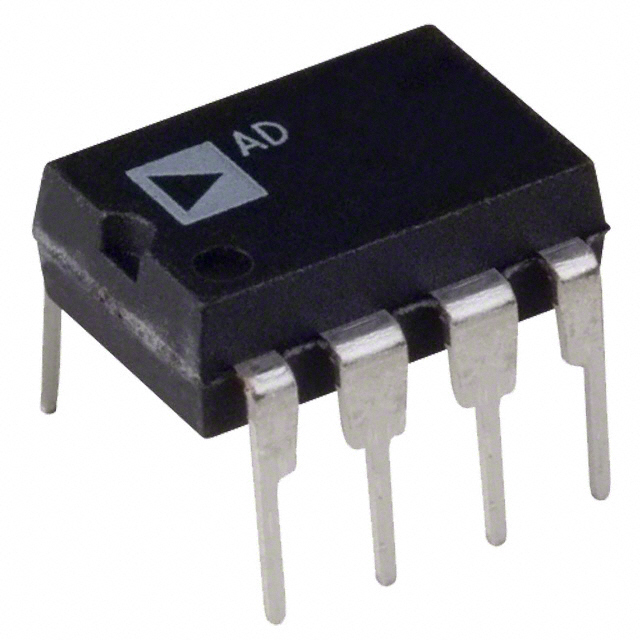
8 Pin SOIC and SOIC PackagesApplicationTransducer Interface
Battery Powered Systems
Data Acquisition Systems
Portable Instrumentation
Motor Control
CommunicationsPinout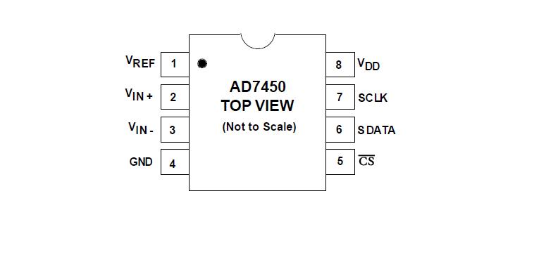
 Specifications
VDD to GND . . . . . . . . . . . . . . . . . . . . . . . .. . . . . . . . . . .-0.3 V to +7 V
VIN+ to GND . . . . . . . . . . . . . . . . .. . . . . . . . . . .0.3 V to VDD + 0.3 V
VIN- to GND . . . . . . . . . . . . . . . . .. . . . . . . . . . . 0.3 V to VDD + 0.3 V
Digital Input Voltage to GND . . .. . . . . . . . . . .. . -0.3 V to VDD + 0.3 V
Digital Output Voltage to GND . .. . . . . . . . . . .. .-0.3 V to VDD + 0.3 V
VREF to GND . . . . . . . . . . . . . . . . . . .. . . . . . . . . .-0.3 V to VDD +0.3 V
Input Current to Any Pin Except Supplies2 . . . .. . . . . . . . . . . . ±10mA
Operating Temperature Range
Commercial (A, B Version) . . . . . . . . .. . . . . . . . . . . . .-40oC to +85oC
Storage Temperature Range . . . . . . . . .. . . . . . . . . . -65oC to +150oC
Junction Temperature . . . . . . . . . . . . . . . . . . . . . . .. . . . . . . . +150oC
SOIC, SOIC Package, Power Dissipation . . . .. . . . . . . . . . . . .450mW
uJA Thermal Impedance . . . . . . . . . .. . . . . . . . . . .. . . .157°C/W (SOIC)
205.9°C/W (SOIC)
uJC Thermal Impedance . . . . . . . . . . .. . . . . . . . . . .. . . .56°C/W (SOIC)
43.74°C/W (SOIC)
Lead Temperature, Soldering
Vapor Phase (60 secs) . . . . . . . . . . . . . . . . . . .. . . . . . . . . . . . . +215oC
Infared (15 secs) . . . . . . . . . . . . . . . . . . . . . . .. . . . . . . . . . . . . .+220oC
ESD . . . . . . . . . . . . . . . . . . . . . . . . . . . . . . . . . . . . . . .. . . . . . . . . . .TBD
| Resolution (Bits) |
12bit |
| T-Put Rate |
1MSPS |
| # Chan |
1 |
| Supply V |
Single(+3),Single(+5) |
| Pwr Diss |
1.3mW |
| Interface |
Ser |
| Ain Range |
(2Vref) p-p |
| SNR (dB) |
n/a |
| Pkg Type |
SOIC,SOP |
DescriptionThe AD7450 is a 12-bit, high speed, low power, successive-approximation (SAR) analog-to-digital converter featuring a fully differential analog input. It operates from a single 3 V or 5 V power supply and features throughput rates up to 833kSPS or 1MSPS respectively.
This part contains a low-noise, wide bandwidth, differential track and hold amplifier (T/H) which can handle input frequencies in excess of 1MHz with the -3dB point being 20MHz typically. The reference voltage for the AD7450 is applied externally to the VREF pin and can be varied from 100 mV to 2.5 V depending on the power supply and to suit the application. The value of the reference voltage determines the common mode voltage range of the part. With this truly differential input structure and variable reference input, the user can select a variety of input ranges and bias points.
The conversion process and data acquisition are controlled using <a href="#" style="text-decoration:overline;">CS</a> and the serial clock allowing the device to interface with Microprocessors or DSPs. The input signals are sampled on the falling edge of <a href="#" style="text-decoration:overline;">CS</a> and the conversion is also initiated at this point.
The SAR architecture of this part ensures that there are no pipeline delays.
The AD7450 uses advanced design techniques to achieve very low power dissipation at high throughput rates.

 AD7450 Data Sheet