Features: · On-Chip Latches for Both DACs
· +5 V to +15 V Operation
· DACs Matched to 1%
· Four Quadrant Multiplication
· TTL/CMOS Compatible
· Latch Free (Protection Schottkys not Required)Application·Digital Control of:
Gain/Attenuation
Filter Parameters
Stereo Audio Circuits
X-Y GraphicsPinout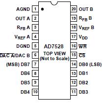
 Specifications
VDD to AGND . . . . . . . . . . . . . . . . . . . . . . . . . . 0 V, +17 V
VDD to DGND . . . . . . . . . . . . . . . . . . . . . . . . . . 0 V, +17 V
AGND to DGND . . . . . . . . . . . . . . . . . . . . . . . . VDD + 0.3 V
DGND to AGND . . . . . . . . . . . . . . . . . . . . . . . . VDD + 0.3 V
Digital Input Voltage to DGND . . . . . . 0.3 V, VDD + 0.3 V
VPIN2, VPIN20 to AGND . . . . . . . . . . . . 0.3 V, VDD + 0.3 V
VREF A, VREF B to AGND . . . . . . . . . . . . . . . . . . . . . . ±25 V
VRFB A, VRFB B to AGND . . . . . . . . . . . . . . . . . . . . . . ±25 V
Power Dissipation (Any Package) to +75°C . . . . . 450 mW
Derates above +75°C by . . . . . . . . . . . . . . . . . . 6 mW/°C
Operating Temperature Range
Commercial (J, K, L) Grades . . . . . . . . . . . 40°C to +85°C
Industrial (A, B, C) Grades . . . . . . . . . . . . 40°C to +85°C
Extended (S, T, U) Grades . . . . . . . . . . . 55°C to +125°C
Storage Temperature . . . . . . . . . . . . . . .65°C to +150°C
Lead Temperature (Soldering, 10 secs) . . . . . . . . .+300°C
CAUTION:
1. ESD sensitive device. The digital control inputs are diode protected; however, permanent damage may occur on unconnected devices subjected to high energy electrostatic fields. Unused devices must be stored in conductive foam or shunts.
2. Do not insert this device into powered sockets. Remove power before insertion or removal.
| Resolution (Bits) |
8bit |
| DAC Update Rate |
5.6MSPS |
| DAC Settling Time |
180ns |
| # DAC Outputs |
2 |
| DAC Type |
Current Out |
| DAC Input Format |
Par |
| Output FSR |
(-Vref),(Bip Vref) |
| Ref Int/Ext |
Ext |
| Supply Vnom |
Single(+15),Single(+5) |
| Pwr Diss |
30mW |
| Package |
DIP,LCC,SOIC |
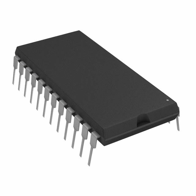
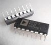
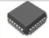
DescriptionThe AD7528 is a monolithic dual 8-bit digital/analog converter featuring excellent DAC-to-DAC matching. It is available in skinny 0.3" wide 20-lead DIPs and in 20-lead surface mount packages.
Separate on-chip latches AD7528 are provided for each DAC to allow easy microprocessor interface.
Data is transferred into either of the two DAC data latches via a common 8-bit TTL/CMOS compatible input port. Control input DAC A/DAC B determines which DAC is to be loaded. The AD7528's load cycle is similar to the write cycle of a random access memory and the device is bus compatible with most 8-bit microprocessors, including 6800, 8080, 8085, Z80.
The device AD7528 operates from a +5 V to +15 V power supply, dissipating only 20 mW of power.
Both DACs AD7528 offer excellent four quadrant multiplication characteristics with a separate reference input and feedback resistor for each DAC.

 AD7528 Data Sheet