Features: Improved Version of AD7541Full Four-Quadrant Multiplication12-Bit Linearity (Endpoint)All Parts Guaranteed MonotonicTTL/CMOS CompatibleLow CostProtection Schottky Diodes Not RequiredLow Logic Input LeakagePinoutSpecifications(TA = +25°C unless otherwise noted)VDD to GND . . . . . . . . ....
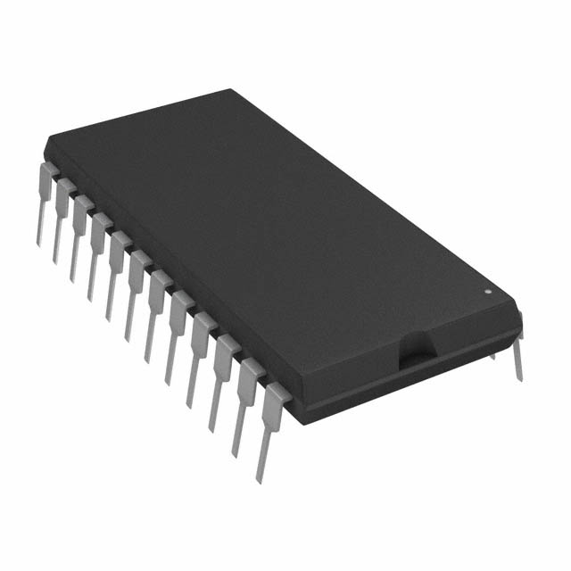
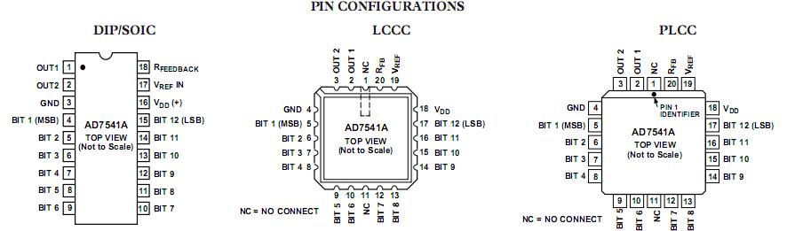
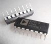
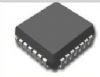
AD7541A: Features: Improved Version of AD7541Full Four-Quadrant Multiplication12-Bit Linearity (Endpoint)All Parts Guaranteed MonotonicTTL/CMOS CompatibleLow CostProtection Schottky Diodes Not RequiredLow Lo...
SeekIC Buyer Protection PLUS - newly updated for 2013!
268 Transactions
All payment methods are secure and covered by SeekIC Buyer Protection PLUS.
(TA = +25°C unless otherwise noted)
VDD to GND . . . . . . . . . . . . . . . . . . . . . . . . . . . . . . . . +17 V
VREF to GND . . . . . . . . . . . . . . . . . . . . . . . . . . . . . . . . ±25 V
VRFB to GND . . . . . . . . . . . . . . . . . . . . . . . . . . . . . . . . . ±25 V
Digital Input Voltage to GND . . . . . . . . 0.3 V, VDD + 0.3 V
OUT 1, OUT 2 to GND . . . . . . . . . . . . 0.3 V, VDD + 0.3 V
Power Dissipation (Any Package)
To +75°C . . . . . . . . . . . . . . . . . . . . . . . . . . . . . . . 450 mW
Derates above +75°C . . . . . . . . . . . . . . . . . . . . . . 6 mW/°C
Operating Temperature Range
Commercial (J, K Versions) . . . . . . . . . . . . . 0°C to +70°C
Industrial (A, B Versions) . . . . . . . . . . . . . 25°C to +85°C
Extended (S, T Versions) . . . . . . . . . . . . . 55°C to +125°C
Storage Temperature . . . . . . . . . . . . . . . . . . 65°C to +150°C
Lead Temperature (Soldering, 10 secs) . . . . . . . . . . . +300°C
The Analog Devices AD7541A is a low cost, high performance 12-bit monolithic multiplying digital-to-analog converter. It is fabricated using advanced, low noise, thin film on CMOS technology and is available in a standard 18-lead DIP and in 20-terminal surface mount packages.
The AD7541A is functionally and pin compatible with the industry standard AD7541 device and offers improved specifications and performance. The improved design ensures that the device is latch-up free so no output protection Schottky diodes are required.