Features: ·16-Bit Monotonicity over Temperature
·±2 LSBs Integral Linearity Error
·Microprocessor Compatible with Readback Capability
·Unipolar or Bipolar Output
·Multiplying Capability
·Low Power (100 mW TypicalPinout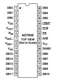
 Specifications
VDD to DGND . . . . . . . . . . . . . . . . . . . . . . . . 0.4 V to +17 V
VCC to DGND . . . . . . . . . . . . . . . 0.4 V, VDD + 0.4 V or +7 V
(Whichever Is Lower)
VSS to DGND . . . . . . . . . . . . . . . . . . . . . . . . . +0.4 V to 17 V
VREF+ to DGND . . . . . . . . . . . . . . . . VDD + 0.4 V, VSS 0.4 V
VREF to DGND . . . . . . . . . . . . . . . . VDD + 0.4 V, VSS 0.4 V
VOUT to DGND2 . . . . . . . . VDD + 0.4 V, VSS 0.4 V or ±10 V
(Whichever Is Lower)
RIN to DGND . . . . . . . . . . . . . . . . . . VDD + 0.4 V, VSS 0.4 V
Digital Input Voltage to DGND . . . . . . 0.4 V to VCC + 0.4 V
Digital Output Voltage to DGND . . . . . 0.4 V to VCC + 0.4 V
Power Dissipation (Any Package)
To +75°C . . . . . . . . . . . . . . . . . . . . . . . . . . . . . . 1000 mW
Derates above +75°C . . . . . . . . . . . . . . . . . . . 10 mW/°C
Operating Temperature Range
J, K Versions . . . . . . . . . . . . . . . . . . . . . . . . 0°C to +70°C
A, B Versions . . . . . . . . . . . . . . . . . . . . . 25°C to +85°C
Storage Temperature Range . . . . . . . . . . 65°C to +150°C
Lead Temperature (Soldering) . . . . . . . . . . . . . . . . . +300°C
NOTES
1 Stresses above those listed under Absolute Maximum Ratings may cause permanent damage to the device. This is a stress rating only; functional operation of the device at these or any other conditions above those indicated in the operational sections of this specification is not implied. Exposure to absolute maximum rating conditions for extended periods may affect device reliability. Only one Absolute Maximum Rating may be applied at any one time.
2 VOUT may be shorted to DGND, VDD, VSS, VCC provided that the power dissipation of the package is not exceeded.
| Resolution (Bits) |
16bit |
| DAC Update Rate |
143kSPS |
| DAC Settling Time |
7s |
| # DAC Outputs |
1 |
| DAC Type |
Voltage Out |
| DAC Input Format |
Par |
| Output FSR |
(-Vref),(Bip 2Vref),(Bip Vref),(Uni 2Vref),(Uni Vref),User Def. Range/Offset |
| Ref Int/Ext |
Ext |
| Supply Vnom |
Multi(±15, +5Dig) |
| Pwr Diss |
155mW |
| Package |
DIP,LCC |
DescriptionThe AD7846 is a 16-bit DAC constructed with Analog Devices'LC2MOS process. It has VREF+ and VREF reference inputs and an on-chip output amplifier. These can be configured to give a unipolar output range (0 V to +5 V, 0 V to +10 V) or bipolar output ranges (±5 V, ±10 V).
The DAC uses a segmented architecture. The 4 MSBs in the DAC latch select one of the segments in a 16-resistor string.Both taps of the segment are buffered by amplifiers and fed to a 12-bit DAC, which provides a further 12 bits of resolution. This architecture ensures 16-bit monotonicity. Excellent integral linearity results from tight matching between the input offset voltages of the two buffer amplifiers.
In addition to the excellent accuracy specifications, the AD7846 also offers a comprehensive microprocessor interface. There are 16 data I/O pins, plus control lines (CS, R/W, LDAC and CLR).R/W andCS allow writing to and reading from the I/O latch.This is the readback function which is useful in ATE applications.LDAC allows simultaneous updating of DACs in a multi-DAC system and theCLR line will reset the contents of the DAC latch to 00 . . . 000 or 10 . . . 000 depending on the state of R/W. This means that the DAC output can be reset to 0 V in both the unipolar and bipolar configurations.
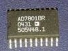
The AD7846 is available in 28-lead plastic, ceramic, and PLCC packages.

 AD7846 Data Sheet