Features: · 14-Bit/16-Bit Multiplying DAC
· Guaranteed Monotonicity
· Output Control on Power-Up and Power-Down
Internal or External Control
· Versatile Serial Interface
· DAC Clears to 0 V in Both Unipolar and Bipolar OutputApplication·Industrial Process Control
·PC Analog I/O Boards
·InstrumentationPinout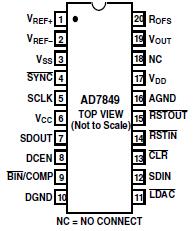
 Specifications
VDD to DGND . . . . . . . . . . . . . . . . . . . . . . . . . 0.4 V to +17 V
VCC to DGND2 . . . . . . . . . . . . . . . . . . 0.4 V, VDD + 0.4 V or
+7 V (Whichever Is Lower)
VSS to DGND . . . . . . . . . . . . . . . . . . . . . . . . . 0.4 V to 17 V
VREF+ to DGND . . . . . . . . . . . . . . . . VDD + 0.4 V, VSS 0.4 V
VREF to DGND . . . . . . . . . . . . . . . . VDD + 0.4 V, VSS 0.4 V
VOUT to DGND3 . . . . . . . . . . . . . .VDD + 0.4 V, VSS 0.4 V or
±10 V (Whichever Is Lower)
ROFS to DGND . . . . . . . . . . . . . . . . . VDD + 0.4 V, VSS 0.4 V
Digital Input Voltage to DGND . . . . . . 0.4 V to VCC + 0.4 V
Input Current to any Pin Except Supplies4 . . . . . . . . . ±10 mA
Operating Temperature Range
Commercial/Industrial (A, B, C Versions). . . . 40°C to +85°C
Extended (T Version) . . . . . . . . . . . . . . . . 55°C to +125°C
Storage Temperature Range . . . . . . . . . . . . 65°C to +150°C
Junction Temperature . . . . . . . . . . . . . . . . . . . . . . . .+150°C
Plastic DIP Package, Power Dissipation . . . . . . . . . . . 875 mW
JA Thermal Impedance . . . . . . . . . . . . . . . . . . . . . 102°C/W
Lead Temperature (Soldering, 10 secs) . . . . . . . . . . +260°C
SOP Package, Power Dissipation . . . . . . . . . . . . . . . . 875 mW
JA Thermal Impedance . . . . . . . . . . . . . . . . . . . . . ..74°C/W
Lead Temperature, Soldering
Vapor Phase (60 secs) . . . . . . . . . . . . . . . . . . . . . . +215°C
Infrared (15 secs) . . . . . . . . . . . . . . . . . . . . . . . . . +220°C
Cerdip Package, Power Dissipation . . . . . . . . . . . . . . 875 mW
JA Thermal Impedance . . . . . . . . . . . . . . . . . . . . . . 71°C/W
Lead Temperature, Soldering (Soldering 10 secs) . . . 260°C
NOTES
1Stresses above those listed under Absolute Maximum Ratings may cause permanent damage to the device. This is a stress rating only; functional operation of the device at these or any other conditions above those listed in the operational sections of this specification is not implied. Exposure to absolute maximum rating conditions for extended periods may affect device reliability.
2VCC must not exceed VDD by more than 0.4 V. If it is possible for this to happen during power-up or power-down (for example, if VCC is greater than +0.4 V while VDD is still 0 V), the following diode protection scheme will ensure rotection.
3VOUT may be shorted to DGND, +10 V, 10 V, provided that the power dissipation of the package is not exceeded.
4Transient currents of up to 100 mA will not cause SCR latch-up.
| Resolution (Bits) |
16bit |
| DAC Update Rate |
143kSPS |
| DAC Settling Time |
7s |
| # DAC Outputs |
1 |
| DAC Type |
Voltage Out |
| DAC Input Format |
Ser |
| Output FSR |
(-Vref),(Bip 2Vref),(Bip Vref),(Uni 2Vref),(Uni Vref),User Def. Range/Offset |
| Ref Int/Ext |
Ext |
| Supply Vnom |
Multi(±15, +5Dig) |
| Pwr Diss |
163mW |
| Package |
DIP,SOIC |
DescriptionThe AD7849 is a 14-bit/16-bit serial input multiplying DAC. The DAC architecture ensures excellent differential linearity performance, and monotonicity is guaranteed to 14 bits for the A grade and to 16 bits for all other grades over the specified temperature ranges.
During power-up and power-down sequences (when the supply voltages are changing), the VOUT pin is clamped to 0 V via a low impedance path. To prevent the output of A3 being shorted to 0 V during this time, transmission gate G1 is also opened. These conditions are maintained until the power supplies stabilize and a valid word is written to the DAC register. At this time, G2 opens and G1 closes. Both transmission gates are also externally controllable via the Reset In (RST IN) control input. For instance, if theRST IN input is driven from a battery supervisor chip, then on power-off or during a brown out, theRST IN input will be driven low to open G1 and close G2. The DAC must be reloaded, withRST IN high, to re-enable the output. Conversely, the on-chip voltage detector output (RST OUT) is also available to the user to control other parts of the system.
The AD7849 has a versatile serial interface structure and can be controlled over three lines to facilitate opto-isolator applications.
SDOUT is the output of the on-chip shift register and can be used in a daisy-chain fashion to program devices in the multichannel system. The DCEN (Daisy Chain Enable) input controls this function.
The BIN/COMP pin sets the DAC coding; with BIN/COMP set to 0, the coding is straight binary; and with it set to 1, the coding is 2s complement. This allows the user to reset the DAC to 0 V in both the unipolar and bipolar output ranges.
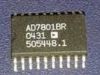
The part is available in a 20-lead DIP and 20-lead SOIC package.

 AD7849 Data Sheet