Features: Two Fast 14-Bit ADCs Four Input Channels Simultaneous Sampling and Conversion 5.2s Conversion Time Single Supply Operation Selection of Input Ranges ±10 V for AD7863-10 ±2.5 V for AD7863-3 0 V to 2.5 V for AD7863-2 High Speed Parallel Interface Low Power, 70 mW Typ Power Saving Mode, 105W Max Overvoltage Protection on Analog Inputs 14-Bit Lead Compatible Upgrade to AD7862
Pinout Specifications
(TA = +25°C unless otherwise noted)
VDD to AGND . . . . . . . . . . . . . . . . . . . . . . . . ............................ 0.3 V to +7 V
VDD to DGND . . . . . . . . . . . . . . . . . . . . . . . . ............................ 0.3 V to +7 V
Analog Input Voltage to AGND
AD7863-10 . . . . . . . . . . . . . . . . . . . . . . . . . . . . . . . . ..............................±17 V
AD7863-3 . . . . . . . . . . . . . . . . . . . . . . . . . . . . . . . . ............................... . ±7 V
AD7863-2 . . . . . . . . . . . . . . . . . . . . . . . . . . . . . . . . . ................................ +7 V
Reference Input Voltage to AGND . . . .............................0.3 V to VDD + 0.3 V
Digital Input Voltage to DGND . . . . . ...............................0.3 V to VDD + 0.3 V
Digital Output Voltage to DGND . . . ................................ 0.3 V to VDD + 0.3 V
Operating Temperature Range
Commercial (A, B Version) . . . . . . . . . . . . ...................................40 to +85
Storage Temperature Range . . . . . . . . . . ................................. 65to +150
Junction Temperature . . . . . . . . . . . . . . . . . . . . . . . ............................... .+150
SOIC Package, Power Dissipation . . . . . . . . . . . . . . .............................. 450 mW
JA Thermal Impedance . . . . . . . . . . . . . . . . . . . ................................... 110/W
Lead Temperature, Soldering
Vapor Phase (60 sec) . . . . . . . . . . . . . . . . . . . . ...................................... .+215
Infrared (15 sec) . . . . . . . . . . . . . . . . . . . . . . . ........................................ .+220
SSOP Package, Power Dissipation . . . . . . . . . . . . ............................... . . 450 mW
JA Thermal Impedance . . . . . . . . . . . . . . . . . . . .................................... 110/W
Lead Temperature, Soldering
Vapor Phase (60 sec) . . . . . . . . . . . . . . . . . . . . ....................................... .+215
Infrared (15 sec) . . . . . . . . . . . . . . . . . . . . . . . ......................................... .+220
*Stresses above those listed under Absolute Maximum Ratings may cause permanent damage to the device. This is a stress rating only; functional operation of the device at these or any other conditions above those listed in the operational sections of this specification is not implied. Exposure to absolute maximum rating conditions for extended periods may affect device reliability.
| Resolution (Bits) |
14bit |
| T-Put Rate |
175kSPS |
| # Chan |
4 |
| Supply V |
Single(+5) |
| Pwr Diss (max) |
52.5mW |
| Interface |
Par |
| Ain Range |
Bip 10V,Bip 2.5V,Uni 2.5V |
| SNR (dB) |
78dB |
| Pkg Type |
SOIC,SOP |
DescriptionThe AD7863 is a high speed, low power, dual 14-bit A/D converter that operates from a single +5 V supply. The part contains two 5.2 s successive approximation ADCs, two track/hold amplifiers, an internal +2.5 V reference and a high speed parallel interface. Four analog inputs are grouped into two channels (A and B) selected by the A0 input. Each channel has two inputs (VA1 and VA2 or VB1 and VB2), which can be sampled and converted simultaneously thus preserving the relative phase information of the signals on both analog inputs. The part accepts an analog input range of ±10 V (AD7863-10), ±2.5 V (AD7863-3) and 0 V2.5 V (AD7863-2). Overvoltage protection on the analog inputs for the part allows the input voltage to go to ±17 V, ±7 V or +7 V respectively, without causing damage.
A single conversion start signal (CONVST) simultaneously places both track/holds into hold and initiates conversion on both channels. The BUSY signal indicates the end of conversion and at this time the conversion results for both channels are available to be read. The first read after a conversion accesses the result from VA1 or VB1, while the second read accesses the result from VA2 or VB2, depending on whether the multiplexer select A0 is low or high respectively. Data is read from the part via a 14-bit parallel data bus with standard CS and RDsignals.
In addition to the traditional dc accuracy specifications such as linearity, gain and offset errors, the part is also specified for dynamic performance parameters including harmonic distortion
and signal-to-noise ratio.
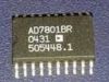
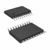
The AD7863 is fabricated in Analog Devices' Linear Compatible CMOS (LC2MOS) process, a mixed technology process that combines precision bipolar circuits with low power CMOS logic. It is available in 28-lead SOIC and SSOP.

 AD7863 Data Sheet