AD7887

Features: Specified for VDDof +2.7V to +5.25VFlexible Power/Throughput Rate ManagementShutdown Mode: 1 A MaxOne/Two Single-Ended InputsSerial Interface: SPI™/QSPI™/MICROWIRE™/DSP Compatible8-Lead Narrow SOIC and SOIC PackagesApplication-Battery-Powered Systems (Personal Digital A...

product image

AD7887 Picture
SeekIC No. : 004271203 Detail

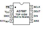
AD7887: Features: Specified for VDDof +2.7V to +5.25VFlexible Power/Throughput Rate ManagementShutdown Mode: 1 A MaxOne/Two Single-Ended InputsSerial Interface: SPI™/QSPI™/MICROWIRE™/DSP C...

floor Price/Ceiling Price

Part Number:
AD7887
Supply Ability:
5000

Price Break

  • Qty
  • 1~5000
  • Unit Price
  • Negotiable
  • Processing time
  • 15 Days
Total Cost: $ 0.00

SeekIC Buyer Protection PLUS - newly updated for 2013!

  • Escrow Protection.
  • Guaranteed refunds.
  • Secure payments.
  • Learn more >>

Month Sales

268 Transactions

Rating

evaluate  (4.8 stars)

Upload time: 2024/4/28

Payment Methods

All payment methods are secure and covered by SeekIC Buyer Protection PLUS.

Notice: When you place an order, your payment is made to SeekIC and not to your seller. SeekIC only pays the seller after confirming you have received your order. We will also never share your payment details with your seller.
Product Details

Description


Features:

Specified for VDDof +2.7V to +5.25V
Flexible Power/Throughput Rate Management
Shutdown Mode: 1 A Max
One/Two Single-Ended Inputs
Serial Interface: SPI™/QSPI™/MICROWIRE™/DSP Compatible
8-Lead Narrow SOIC and SOIC Packages


Application

-Battery-Powered Systems (Personal Digital Assistants,Medical Instruments, Mobile Communications)
-Instrumentation and Control Systems
-High Speed Modems


-Battery-Powered Systems (Personal Digital Assistants,Medical Instruments, Mobile Communications)
-Instrumentation and Control Systems
-High Speed Modems


Pinout

  Connection Diagram


Specifications

(TA= +25°C unless otherwise noted)
VDDto AGND . . . . . . . . . . . . . . . . . . . . . . . .0.3 V to +7 V
Analog Input Voltage to AGND . . . . .0.3 V to VDD+ 0.3 V
Digital Input Voltage to AGND . . . . .0.3 V to VDD+ 0.3 V
Digital Output Voltage to AGND . . . .0.3 V to VDD+ 0.3 V
REFIN/REFOUTto AGND . . . . . . . . . .0.3 V to VDD+ 0.3 V
Input Current to Any Pin Except Supplies2. . . . . . .±10 mA
Operating Temperature Range
Commercial
A, B Versions . . . . . . . . . . . . . . . . . . . .40°C to +125°C
Storage Temperature Range . . . . . ... .65°C to +150°C
Junction Temperature . . . . . . . . . . . . . . . . . . . . ..+150°C
SOIC, µSOIC Package, Power Dissipation . . . . . .450 mW
JAThermal Impedance . . . . . . . . . .. . .157°C/W (SOIC)
. . . . . . . . . . . . . . . . . . . . . . . . . . . . .205.9°C/W (µSOIC)
JCThermal Impedance . . . . . . . . . .. . . .56°C/W (SOIC)
. . . . . . . . . . . . . . . . . . . . . . . . . . . . .43.74°C/W (µSOIC)
Lead Temperature, Soldering
Vapor Phase (60 sec) . . . . . . . . . . . . . . . . . . . . . .+215°C
Infrared (15 sec) . . . . . . . . . . . . . . . . . . . . . . . . . .+220°C
ESD . . . . . . . . . . . . . . . . . . . . . . . . . . . . . . . . . . . . . .4.5 kV


Resolution (Bits) 12bit
T-Put Rate 125kSPS
# Chan 2
Supply V Single(+3),Single(+3.3),Single(+5)
Pwr Diss 3.5mW
Interface Ser,SPI
Ain Range Uni (Vref)
SNR (dB) 71dB
Pkg Type SOIC,SOP


Description

The AD7887 is a high speed, low power, 12-bit ADC that oper-ates from a single +2.7 V to +5.25 V power supply. The AD7887 is capable of 125 kSPS throughput rate. The input track-and- hold acquires a signal in 500 ns and features a single-ended sampling scheme. The output coding for the AD7887 is straight binary and the part is capable of converting full power signals up to 2.5 MHz.

The AD7887 can be configured for either dual or single chan-nel operation, via the on-chip Control Register. There is a default single-channel mode that allows the AD7887 to be operated as a read-only ADC. In single-channel operation, there is one analog input (AIN0) with the V REF/AIN1 pin as-suming its VREFfunction. This VREFpin allows the user access to the part's internal +2.5 V reference, or the VREFpin can be overdriven by an external reference to provide the reference voltage for the part. This external reference voltage has a range of +2.5 V to VDD. The analog input range on AIN0 is 0 to +VREF.

In dual-channel operation, the VREF/AIN1 pin assumes its AIN1 function, providing a second analog input channel. In this case, the reference voltage for the part is provided via the VDD pin. As a result, the input voltage range on both the AIN0 and AIN1 inputs is 0 to VDD.


Customers Who Bought This Item Also Bought

Margin,quality,low-cost products with low minimum orders. Secure your online payments with SeekIC Buyer Protection.
Line Protection, Backups
Sensors, Transducers
Potentiometers, Variable Resistors
Power Supplies - Board Mount
RF and RFID
Optical Inspection Equipment
View more