AD7904

Features: Fast Throughput Rate: 1 MSPSSpecified for VDD of 2.7 V to 5.25 VLow Power:6 mW max at 1 MSPS with 3 V Supplies13.5 mW max at 1 MSPS with 5 V Supplies4 (Single-Ended) Inputs with SequencerWide Input Bandwidth:AD7924, 70 dB SNR at 50 kHz Input FrequencyFlexible Power/Serial Clock Speed Man...

product image

AD7904 Picture
SeekIC No. : 004271288 Detail

AD7904: Features: Fast Throughput Rate: 1 MSPSSpecified for VDD of 2.7 V to 5.25 VLow Power:6 mW max at 1 MSPS with 3 V Supplies13.5 mW max at 1 MSPS with 5 V Supplies4 (Single-Ended) Inputs with SequencerW...

floor Price/Ceiling Price

Part Number:
AD7904
Supply Ability:
5000

Price Break

  • Qty
  • 1~5000
  • Unit Price
  • Negotiable
  • Processing time
  • 15 Days
Total Cost: $ 0.00

SeekIC Buyer Protection PLUS - newly updated for 2013!

  • Escrow Protection.
  • Guaranteed refunds.
  • Secure payments.
  • Learn more >>

Month Sales

268 Transactions

Rating

evaluate  (4.8 stars)

Upload time: 2024/4/18

Payment Methods

All payment methods are secure and covered by SeekIC Buyer Protection PLUS.

Notice: When you place an order, your payment is made to SeekIC and not to your seller. SeekIC only pays the seller after confirming you have received your order. We will also never share your payment details with your seller.
Product Details

Description


Features:

Fast Throughput Rate: 1 MSPS
Specified for VDD of 2.7 V to 5.25 V
Low Power:
6 mW max at 1 MSPS with 3 V Supplies
13.5 mW max at 1 MSPS with 5 V Supplies
4 (Single-Ended) Inputs with Sequencer
Wide Input Bandwidth:
AD7924, 70 dB SNR at 50 kHz Input Frequency
Flexible Power/Serial Clock Speed Management
No Pipeline Delays
High Speed Serial Interface SPITM /QSPITM /
MICROWIRE TM/DSP Compatible
Shutdown Mode: 0.5 A Max
16-Lead TSSOP Package


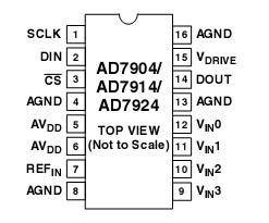
Pinout

  Connection Diagram


Specifications

AVDD to AGND ................................................................... 0.3 V to +7 V
VDRIVE to AGND.................................................... 0.3 V to AVDD + 0.3 V
Analog Input Voltage to AGND ............................. 0.3 V to AVDD + 0.3 V
Digital Input Voltage to AGND............................................ 0.3 V to +7 V
Digital Output Voltage to AGND............................ 0.3 V to AVDD + 0.3 V
REFIN to AGND...................................................... 0.3 V to AVDD + 0.3 V
Input Current to Any Pin Except Supplies2 .................................. ±10 mA
Operating Temperature Range
Commercial (B Version) ................................................ 40°C to +85°C
Storage Temperature Range.......................................65°C to +150°C
Junction Temperature ........................................... ....................... 150°C
TSSOP Package, Power Dissipation ............................................. 450 mW
JA Thermal Impedance.......................... ...................150.4°C/W (TSSOP)
JC Thermal Impedance....................... ....................... 27.6°C/W (TSSOP)
Lead Temperature, Soldering
Vapor Phase (60 secs) .............................. .................................. 215°C
Infrared (15 secs)......................................................................... 220°C
ESD.................................................................................................... 2 kV


Resolution (Bits) 8bit
T-Put Rate 1MSPS
# Chan 4
Supply V Single(+3),Single(+3.3),Single(+5)
Pwr Diss 13.5mW
Interface Ser,SPI
Ain Range Uni (Vref),Uni (Vref) x 2
SNR (dB) 49dB
Pkg Type SOP


Description

The AD7904/AD7914/AD7924 are respectively, 8-bit, 10-bit,and 12-bit, high speed, low power, 4-channel, successive-approxi-mation ADCs. The parts operate from a single 2.7 V to 5.25 V
power supply and feature throughput rates up to 1 MSPS. The parts contain a low noise, wide bandwidth track/hold amplifier that can handle input frequencies in excess of 8 MHz.

The conversion process and data acquisition are controlled using CS and the serial clock signal, allowing the device to easily interface with microprocessors or DSPs. The input signal is sampled on the falling edge of CS and conversion is also initiated at this point. There are no pipeline delays associated with the part.

The AD7904/AD7914/AD7924 use advanced design techniques to achieve very low power dissipation at maximum throughput rates. At maximum throughput rates, the AD7904/AD7914/AD7924 consume 2 mA maximum with 3 V supplies; with 5 V supplies, the current consumption is 2.7 mA maximum.

Through the configuration of the Control Register, the analog input range for the part can be selected as 0 V to REFIN or 0 V to 2 × REFIN, with either straight binary or twos complement
output coding. The AD7904/AD7914/AD7924 each feature four single-ended analog inputs with a channel sequencer to allow a preprogrammed selection of channels to be converted sequentially.

The conversion time for the AD7904/AD7914/AD7924 is deter- mined by the SCLK frequency, as this is also used as the master clock to control the conversion.


Customers Who Bought This Item Also Bought

Margin,quality,low-cost products with low minimum orders. Secure your online payments with SeekIC Buyer Protection.
Power Supplies - Board Mount
Semiconductor Modules
Optical Inspection Equipment
Static Control, ESD, Clean Room Products
Prototyping Products
DE1
Crystals and Oscillators
View more