AD8251

Features: `Small package: 10-lead MSOP`Programmable gains: 1, 2, 4, 8`Digital or pin-programmable gain setting`Wide supply: ±5 V to ±15 V`Excellent dc performanceHigh CMRR 96 dB (min), G = 8Low gain drift: 10 ppm/°C (max)Low offset drift: 1.8 V/°C (max), G = 8`Excellent ac performanceFast settling...

product image

AD8251 Picture
SeekIC No. : 004271988 Detail

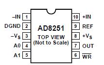
AD8251: Features: `Small package: 10-lead MSOP`Programmable gains: 1, 2, 4, 8`Digital or pin-programmable gain setting`Wide supply: ±5 V to ±15 V`Excellent dc performanceHigh CMRR 96 dB (min), G = 8Low gain...

floor Price/Ceiling Price

Part Number:
AD8251
Supply Ability:
5000

Price Break

  • Qty
  • 1~5000
  • Unit Price
  • Negotiable
  • Processing time
  • 15 Days
Total Cost: $ 0.00

SeekIC Buyer Protection PLUS - newly updated for 2013!

  • Escrow Protection.
  • Guaranteed refunds.
  • Secure payments.
  • Learn more >>

Month Sales

268 Transactions

Rating

evaluate  (4.8 stars)

Upload time: 2024/4/24

Payment Methods

All payment methods are secure and covered by SeekIC Buyer Protection PLUS.

Notice: When you place an order, your payment is made to SeekIC and not to your seller. SeekIC only pays the seller after confirming you have received your order. We will also never share your payment details with your seller.
Product Details

Description


Features:

`Small package: 10-lead MSOP
`Programmable gains: 1, 2, 4, 8
`Digital or pin-programmable gain setting
`Wide supply: ±5 V to ±15 V
`Excellent dc performance
High CMRR 96 dB (min), G = 8
Low gain drift: 10 ppm/°C (max)
Low offset drift: 1.8 V/°C (max), G = 8
`Excellent ac performance
Fast settling time: 615 ns to 0.001% (max)
High slew rate: 20 V/s (min)
Low distortion: −110 dB THD at 1 kHz
High CMRR over frequency: 80 dB to 50 kHz (min)
Low noise: 18 nV/Hz, G = 8 (max)
Low power: 4 mA


Application

·Data acquisition
·Biomedical analysis
·Test and measurement


Pinout

AD8251 Diagram

  Connection Diagram


Specifications

Single/Dual Supply Dual
Gain Setting Method Pin,Software
Gain Range (min to max) 8
Bandwidth G=10 (kHz typ) 2500kHz
CMRR (dB) 98dB
Vnoise RTI 1-10 Hz Vp-p 1.2V p-p
Temperature Range -40 to +85
Supply Current 3.5mA


Parameter Rating
Supply Voltage ±17 V
Power Dissipation See Figure 3
Output Short-Circuit Current Indefinite1
Common-Mode Input Voltage ±VS
Differential Input Voltage ±VS
Digital Logic Inputs ±VS
Storage Temperature Range 65°C to +125°C
Operating Temperature Range2 40°C to +85°C
Lead Temperature (Soldering 10 sec) 300°C
Junction Temperature 140°C
JA (4-Layer JEDEC Standard Board) 112°C/W
Package Glass Transition Temperature 140°C
1 Assumes the load is referenced to mid supply.
2 Temperature for specified performance is −40°C to +85°C..

Stresses above those listed under Absolute Maximum Ratings may cause permanent damage to the device. This is a stress rating only; functional operation of the device at these or any other conditions above those indicated in the operational section of this specification is not implied. Exposure to absolute maximum rating conditions for extended periods may affect device reliability.


Description

The AD8251 is an instrumentation amplifier with digitally programmable gains that has G input impedance, low output noise, and low distortion making it suitable for interfacing with sensors and driving high sample rate analog-to-digital converters (ADCs). It has high bandwidth of 10 MHz, low THD of −110 dB and fast settling time of 615 ns to 0.001%. Offset drift and gain drift are guaranteed to 1.8 V/°C and 10 ppm/°C, respectively for G = 8. In addition to its wide input common voltage range, it boasts a high common-mode rejection of 80 dB at G = 1 from dc to 50 kHz. The combination of precision dc performance coupled with high speed capabilities make the AD8251 an excellent candidate for data acquisition. Furthermore, this monolithic solution simplifies design and manufacturing, and boosts performance of instrumentation by maintaining a tight match of internal resistors and amplifiers.

The AD8251 user interface consists of a parallel port that allows users to set the gain in one of two different ways (see Figure 1 for the functional block diagram). A 2-bit word sent via a bus can be latched using theWR input. An alternative is to use transparent gain mode where the state of logic levels at the gain port determines the gain.


Customers Who Bought This Item Also Bought

Margin,quality,low-cost products with low minimum orders. Secure your online payments with SeekIC Buyer Protection.
Sensors, Transducers
Integrated Circuits (ICs)
Potentiometers, Variable Resistors
Motors, Solenoids, Driver Boards/Modules
Optical Inspection Equipment
View more