AD8600

Features: `16 Independently Addressable Voltage Outputs`Full-Scale Set by External Reference`2 s Settling Time`Double Buffered 8-Bit Parallel Input`High Speed Data Load Rate`Data Readback`Operates from Single +5 V`Optional ±6 V Supply Extends Output RangeApplication·Phased Array Ultrasound & S...

product image

AD8600 Picture
SeekIC No. : 004272536 Detail

AD8600: Features: `16 Independently Addressable Voltage Outputs`Full-Scale Set by External Reference`2 s Settling Time`Double Buffered 8-Bit Parallel Input`High Speed Data Load Rate`Data Readback`Operates f...

floor Price/Ceiling Price

Part Number:
AD8600
Supply Ability:
5000

Price Break

  • Qty
  • 1~5000
  • Unit Price
  • Negotiable
  • Processing time
  • 15 Days
Total Cost: $ 0.00

SeekIC Buyer Protection PLUS - newly updated for 2013!

  • Escrow Protection.
  • Guaranteed refunds.
  • Secure payments.
  • Learn more >>

Month Sales

268 Transactions

Rating

evaluate  (4.8 stars)

Upload time: 2024/4/18

Payment Methods

All payment methods are secure and covered by SeekIC Buyer Protection PLUS.

Notice: When you place an order, your payment is made to SeekIC and not to your seller. SeekIC only pays the seller after confirming you have received your order. We will also never share your payment details with your seller.
Product Details

Description


Features:

`16 Independently Addressable Voltage Outputs
`Full-Scale Set by External Reference
`2 s Settling Time
`Double Buffered 8-Bit Parallel Input
`High Speed Data Load Rate
`Data Readback
`Operates from Single +5 V
`Optional ±6 V Supply Extends Output Range


Application

·Phased Array Ultrasound & Sonar
·Power Level Setting
·Receiver Gain Setting
·Automatic Test Equipment
·LCD Clock Level Setting


Pinout

  Connection Diagram


Specifications

VDD1 (Digital Supply) to GND . . . . . . . . . . . . . . 0.3 V, +7 V
VDD2 (DAC Buffer/Driver Supply) . . . . . . . . . . . . 0.3 V, +7 V
VCC (Analog Supply) to GND . . . . . . . . . . . . . . . 0.3 V, +7 V
VEE (Analog Supply) to GND . . . . . . . . . . . . . . . +0.3 V, 7 V
VREF to GND . . . . . . . . . . . . . . . . . . . . . . 0.3 V, VCC + 0.3 V
VDD2 to VREF . . . . . . . . . . . . . . . . . . . . . . . . . . . . . . . . .0.3 V
VOUT to GND . . . . . . . . . . . . . . . . . . . . . . . . . . . . . . . . . VCC
Short Circuit Duration
VOUT to GND or Power Supplies1
. . . . . . . . . . . . . . . Continuous
Digital Input/Output Voltage to GND . . . 0.3 V, VDD + 0.3 V
Thermal ResistanceTheta Junction-to-Ambient (JA)
PLCC-44 . . . . . . . . . . . . . . . . . . . . . . . . . . . . . . . . 47/W
Package Power Dissipation . . . . . . . . . . . . . . . . (TJ TA)/JA
Maximum Junction Temperature TJ max . . . . . . . . . . . 150
Operating Temperature Range . . . . . . . . . . . . 40 to +85
Storage Temperature Range . . . . . . . . . . . . 65 to +150
Lead Temperature (Soldering, 10 sec) . . . . . . . . . . . . +300


Description

The AD8600 contains 16 independent voltage output digital-toanalog converters that share a common external reference input voltage. Each DAC has its own DAC register and input register to allow double buffering. An 8-bit parallel data input, four address pins, a CS select, a LD , EN, R  Connection Diagram
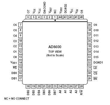
, and RS provide the digital interface.

The AD8600 is constructed in a monolithic CBCMOS process which optimizes use of CMOS for logic and bipolar for speed and precision. The digital-to-analog converter design uses voltage mode operation ideally suited to single supply operation. The internal DAC voltage range is fixed at DACGND to VREF. The voltage buffers provide an output voltage range that approaches ground and extends to 1.0 V below VCC. Changes in reference voltage values and digital inputs will settle within ±1 LSB in 2 ms.

Data is preloaded into the input registers one at a time after the internal address decoder selects the input register. In the write mode (R  Connection Diagram low) data is latched into the input register during the positive edge of the EN pulse. Pulses as short as 40 ns can be used to load the data. After changes have been submitted to the input registers, the DAC registers are simultaneously updated by a common load EN * LD strobe. The new analog output voltages simultaneously appear on all 16 outputs.

At system power up or during fault recovery the reset (RS ) pin forces all DAC registers into the zero state which places zero volts at all DAC outputs.

The AD8600 is offered in the PLCC-44 package. The device is designed and tested for operation over the extended industrial temperature range of 40°C to +85.


Customers Who Bought This Item Also Bought

Margin,quality,low-cost products with low minimum orders. Secure your online payments with SeekIC Buyer Protection.
Cables, Wires - Management
Line Protection, Backups
Cables, Wires
Circuit Protection
Industrial Controls, Meters
Integrated Circuits (ICs)
View more