AD9411

Features: SNR = 60 dB @ fIN up to 70 MHz @ 200 MSPS ENOB of 9.8 @ fIN up to 70 MHz @ 200 MSPS (0.5 dBFS) SFDR = 80 dBc @ fIN up to 70 MHz @ 200 MSPS (0.5 dBFS) Excellent linearity:DNL = ±0.15 LSB (typical)INL = ±0.25 LSB (typical) LVDS output levels 700 MHz full-power analog bandwidth On-chip ref...

product image

AD9411 Picture
SeekIC No. : 004273077 Detail

AD9411: Features: SNR = 60 dB @ fIN up to 70 MHz @ 200 MSPS ENOB of 9.8 @ fIN up to 70 MHz @ 200 MSPS (0.5 dBFS) SFDR = 80 dBc @ fIN up to 70 MHz @ 200 MSPS (0.5 dBFS) Excellent linearity:DNL = ±0.15 LSB (...

floor Price/Ceiling Price

Part Number:
AD9411
Supply Ability:
5000

Price Break

  • Qty
  • 1~5000
  • Unit Price
  • Negotiable
  • Processing time
  • 15 Days
Total Cost: $ 0.00

SeekIC Buyer Protection PLUS - newly updated for 2013!

  • Escrow Protection.
  • Guaranteed refunds.
  • Secure payments.
  • Learn more >>

Month Sales

268 Transactions

Rating

evaluate  (4.8 stars)

Upload time: 2024/4/17

Payment Methods

All payment methods are secure and covered by SeekIC Buyer Protection PLUS.

Notice: When you place an order, your payment is made to SeekIC and not to your seller. SeekIC only pays the seller after confirming you have received your order. We will also never share your payment details with your seller.
Product Details

Description


Features:

SNR = 60 dB @ fIN up to 70 MHz @ 200 MSPS
ENOB of 9.8 @ fIN up to 70 MHz @ 200 MSPS (0.5 dBFS)
SFDR = 80 dBc @ fIN up to 70 MHz @ 200 MSPS (0.5 dBFS)
Excellent linearity:
DNL = ±0.15 LSB (typical)
INL = ±0.25 LSB (typical)
LVDS output levels
700 MHz full-power analog bandwidth
On-chip reference and track-and-hold
Power dissipation = 1.25 W typical @ 200 MSPS
1.5 V input voltage range
3.3 V supply operation
Output data format option
Clock duty cycle stabilizer
Pin compatible to LVDS mode AD9430


Application

Wireless and wired broadband communications
Cable reverse path
Communications test equipment
Radar and satellite subsystems
Power amplifier linearization


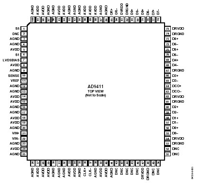
Pinout

  Connection Diagram


Specifications

Parameter Rating
AVDD, DRVDD
Analog Inputs
Digital Inputs
REFIN Inputs
Digital Output Current
Operating Temperature
Storage Temperature
Maximum Junction Temperature
Maximum Case Temperature
JA1
4 V
0.5 V to AVDD +0.5 V
0.5 V to DRVDD +0.5 V
0.5 V to AVDD +0.5 V
20 mA
55ºC to +125°C
65ºC to +150°C
150°C
150°C
25°C/W, 32°C/W


Resolution (Bits) 10bit
T-Put Rate 170MSPS
# Chan 1
Supply V Single(+3),Single(+3.3)
Pwr Diss 1.43W
Interface LVDS,Par
Ain Range 1.5 V p-p
SNR (dB) 60.2dB
Pkg Type QFP


Description

The AD9411 is a 10-bit monolithic sampling analog-to-digital converter optimized for high performance, low power, and ease of use. The product operates up to a 200 MSPS conversion rate and is optimized for outstanding dynamic performance in wideband carrier and broadband systems. All necessary functions, including track-and-hold (T/H) and reference, are included on the chip to provide a complete conversion solution.

The ADC AD9411 requires a 3.3 V power supply and a differential sample clock for full performance operation. The digital outputs are LVDS compatible and support both twos complement and offset binary format. A data clock output is available to ease data capture.

Fabricated on an advanced BiCMOS process, the AD9411 is available in a 100-lead surface-mount plastic package (e-PAD TQFP-100) specified over the industrial temperature range (40°C to +85°C).


Customers Who Bought This Item Also Bought

Margin,quality,low-cost products with low minimum orders. Secure your online payments with SeekIC Buyer Protection.
Optoelectronics
Audio Products
LED Products
Sensors, Transducers
Line Protection, Backups
View more