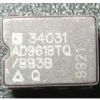
Pinout Specifications
| Resolution (Bits) |
10bit |
| T-Put Rate |
250MSPS |
| # Chan |
1 |
| Supply V |
Multi(+1.8Anlg, +1.8Dig) |
| Pwr Diss |
344MW |
| Interface |
Par |
| Ain Range |
1 V p-p,1.25 V p-p,1.5 V p-p |
| SNR (dB) |
59.4dB |
| Pkg Type |
CSP |
DescriptionThe AD9601 is a 10-bit monolithic sampling analog-to-digital converter optimized for high performance, low power, and ease of use. The product operates at up to a 250 MSPS conversion rate and is optimized for outstanding dynamic performance in wideband carrier and broadband systems. All necessary functions,including a track-and-hold (T/H) and voltage reference,are included on the chip to provide a complete signal conversion solution.
Features of the AD9601 are:(1)single data port at up to 250 MHz; (2)demultiplexed dual port at up to 2 * 125 MHz; (3)700 MHz full power analog bandwidth; (4)on-chip reference, no external decoupling required; (5)integrated input buffer and track-and-hold; (6)1.8 V analog and digital supply operation; (7)selectable output data format (offset binary, twos complement, gray code); (8)clock duty cycle stabilizer; (9)integrated data capture clock.The ADC requires a 1.8 V analog voltage supply and a differential clock for full performance operation. The digital outputs are CMOS compatible and support either twos complement, offset binary format, or Gray code. A data clock output is available for proper output data timing.
The absolute maximum ratings of the AD9601 can be summarized as:(1)AVDD to AGND:-0.3 V to +2.0 V;(2)storage temperature range:-65 to +125;(3)DRVDD to DRGND:-0.3 V to +2.0 V;(4)junction temperature:+150;(5)AVDD to DRVDD:-2.0 V to +2.0 V;(6)CSB to AGND:-0.3 V to +3.6 V.Stresses above those listed under Absolute Maximum Ratings may cause permanent damage to the device. This is a stress rating only; functional operation of the device at these or any other conditions above those indicated in the operational section of this specification is not implied.Exposure to absolute maximum rating conditions for extended periods may affect device reliability.Each stage of the pipeline, excluding the last, consists of a low resolution flash ADC connected to a switched capacitor DAC and interstage residue amplifier (MDAC). The residue amplifier magnifies the difference between the reconstructed DAC output and the flash input for the next stage in the pipeline. One bit of redundancy is used in each stage to facilitate digital correction of flash errors. The last stage simply consists of a flash ADC.

 AD9601 Data Sheet