Features: 180 MHz Clock Rate with Selectable 63 Reference Clock Multiplier
On-Chip High Performance 10-Bit DAC and High Speed Comparator with Hysteresis
SFDR >43 dB @ 70 MHz AOUT
32-Bit Frequency Tuning Word
Simplified Control Interface: Parallel or Serial
Asynchronous Loading Format 5-Bit Phase Modulation and Offset Capability
Comparator Jitter <80 ps p-p @ 20 MHz +2.7 V to +5.25 V Single Supply Operation
Low Power: 555 mW @ 180 MHz
Power-Down Function, 4 mW @ +2.7 V
Ultrasmall 28-Lead SSOP PackagingApplicationFrequency/Phase-Agile Sine Wave Synthesis
Clock Recovery and Locking Circuitry for Digital
Communications
Digitally Controlled ADC Encode Generator
Agile L.O. Applications in Communications
Quadrature Oscillator
CW, AM, FM, FSK, MSK Mode TransmitterPinout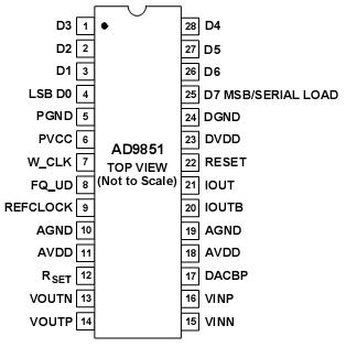
 SpecificationsMaximum Junction Temperature . . . . . . . . . . . . . . . .+150
Storage Temperature . . . . . . . . . . . . . . . . .65 to +150
VS . . . . . . . . . . . . . . . . . . . . . . . . . . . . . . . . . . . . . . . . .+6 V
Operating Temperature . . . . . . . . . . . . . . . .40 to +85
Digital Inputs . . . . . . . . . . . . . . . . . . 0.7 V to +VS + 0.7 V
Lead Temperature (10 sec) Soldering . . . . . . . . . . . +300
Digital Output Current . . . . . . . . . . . . . . . . . . . . . . . 30 mA
SSOP JA Thermal Impedance . . . . . . . . . . . . . . . . . . 82 /W
DAC Output Current . . . . . . . . . . . . . . . . . . . . . . . . ..30 mA
| Compliance Range (V) |
1V |
| FS Iout (mA nom) |
10mA |
| I Supply total (max) |
1210mA |
| I/O Interface |
Parallel,Serial |
| Master fclk |
300MHz |
| Nominal Supply (V) |
Single(+3.3) |
| On-Board Comparator |
Yes |
| REFCLK Multiplier |
Yes |
| Resolution (Bits) |
12bit |
DescriptionThe AD9851 is a highly integrated device that uses advanced DDS technology, coupled with an internal high speed, high performance D/A converter, and comparator, to form a digitally-
programmable frequency synthesizer and clock generator func-tion. When referenced to an accurate clock source, the AD9851 generates a stable frequency and phase-programmable digitized analog output sine wave. This sine wave can be used directly as a frequency source, or internally converted to a square wave for agile-clock generator applications. The AD9851's innovative high speed DDS core accepts a 32-bit frequency tuning word, which results in an output tuning resolution of approximately 0.04 Hz with a 180 MHz system clock. The AD9851 contains a unique 6` REFCLK Multiplier circuit that eliminates the need for a high speed reference oscillator. The 6` REFCLK Multiplier has minimal impact on SFDR and phase noise characteristics.
The AD9851 provides five bits of programmable phase modula-tion resolution to enable phase shifting of its output in incre-ments of 11.25 .
The AD9851 contains an internal high speed comparator that can be configured to accept the (externally) filtered output of the DAC to generate a low jitter output pulse.The frequency tuning, control and phase modulation words are asynchronously loaded into the AD9851 via parallel or serial loading format. The parallel load format consists of five itera-tive loads of an 8-bit control word (byte). The first 8-bit byte controls output phase, 6` REFCLK Multiplier, power-down enable and loading format; the remaining bytes comprise the 32-bit frequency tuning word. Serial loading is accomplished via a 40-bit serial data stream entering through one of the parallel input bus lines. The AD9851 uses advanced CMOS technology to provide this breakthrough level of functionality on just 555 mW of power dissipation (+5 V supply), at the maximum clock rate of 180 MHz.
The AD9851 is available in a space-saving 28-lead SSOP, sur-face mount package that is pin-for-pin compatible with the popular AD9850 125 MHz DDS. It is specified to operate over the extended industrial temperature range of 40 C to +85 C at >3.0 V supply voltage. Below 3.0 V, the specifications apply over the commercial temperature range of 0 C to +85 C.

 AD9854 Data Sheet