AD9864

Features: 10 MHz to 300 MHz input frequency 6.8 kHz to 270 kHz output signal bandwidth 7.5 dB SSB NF 7.0 dBm IIP3 AGC free range up to 34 dBm 12 dB continuous AGC range 16 dB front end attenuator Baseband I/Q 16-bit (or 24-bit) serial digital output LO and sampling clock synthesizers Programmable ...

product image

AD9864 Picture
SeekIC No. : 004273602 Detail

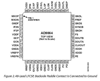
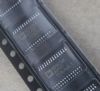
AD9864: Features: 10 MHz to 300 MHz input frequency 6.8 kHz to 270 kHz output signal bandwidth 7.5 dB SSB NF 7.0 dBm IIP3 AGC free range up to 34 dBm 12 dB continuous AGC range 16 dB front end attenuator Ba...

floor Price/Ceiling Price

Part Number:
AD9864
Supply Ability:
5000

Price Break

  • Qty
  • 1~5000
  • Unit Price
  • Negotiable
  • Processing time
  • 15 Days
Total Cost: $ 0.00

SeekIC Buyer Protection PLUS - newly updated for 2013!

  • Escrow Protection.
  • Guaranteed refunds.
  • Secure payments.
  • Learn more >>

Month Sales

268 Transactions

Rating

evaluate  (4.8 stars)

Upload time: 2024/4/27

Payment Methods

All payment methods are secure and covered by SeekIC Buyer Protection PLUS.

Notice: When you place an order, your payment is made to SeekIC and not to your seller. SeekIC only pays the seller after confirming you have received your order. We will also never share your payment details with your seller.
Product Details

Description


Features:

10 MHz to 300 MHz input frequency
6.8 kHz to 270 kHz output signal bandwidth
7.5 dB SSB NF
7.0 dBm IIP3
AGC free range up to 34 dBm
12 dB continuous AGC range
16 dB front end attenuator
Baseband I/Q 16-bit (or 24-bit) serial digital output
LO and sampling clock synthesizers
Programmable decimation factor, output format,
AGC, and sythesizer settings
370 input impedance
2.7 V to 3.6 V supply voltage
Low current consumption: 17 mA
48-lead LFCSP package


Application

Multimode narrow-band radio products
Analog/digital UHF/VHF FDMA receivers
TETRA, APCO25, GSM/EDGE
Portable and mobile radio products
SATCOM terminals


Pinout

AD9864 Diagram

  Connection Diagram


Specifications

Resolution (Bits) 24bit
T-Put Rate 375kSPS
# Chan 1
Supply V Single(+3),Single(+3.3)
Pwr Diss n/a
Interface Ser,SPI
SNR (dB) n/a
Pkg Type CSP


Parameter With Respectto Min Max Unit
VDDF, VDDA, VDDC,
VDDD, VDDH, VDDL, VDDI
VDDF, VDDA, VDDC,
VDDD, VDDH, VDDL, VDDI
VDDP, VDDQ
GNDF, GNDA, GNDC, GNDD,
GNDH, GNDL, GNDI, GNDQ, GNDP, GNDS
MXOP, MXON, LOP,
LON, IFIN, CXIF, CXVL, CXVM
PC, PD, PE, CLKOUT,
DOUTA, DOUTB, FS, SYNCB
IF2N, IF2P, GCP, GCN
VFEFP, VREGN, RREF
IOUTC
IOUTL
CLKP, CLKN
FREF
Junction Temperature
Storage Temperature
Lead Temperature

GNDF, GNDA, GNDC, GNDD,
GNDH, GNDL, GNDI, GNDS
VDDR, VDDA, VDDC,
VDDD, VDDH, VDDL, VDDI
GNDP, GNDQ
GNDF, GNDA, GNDC, GNDD,
GNDH, GNDL, GNDI, GNDQ, GNDP, GNDS
GNDH

GNDH

GNDF
GNDA
GNDQ
GNDP
GNDC
GNDL

0.3

4.0

0.3
0.3

0.3

0.3
0.3
0.3
0.3
0.3
0.3
0.3

65

+4.0
+4.0
+6.0
+0.3

VDDI + 0.3

VDDH + 0.3

VDDF + 0.3
VDDA + 0.3
VDDQ + 0.3
VDDP + 0.3
VDDC + 0.3
VDDL + 0.3
150
+150
300

V

V
V

V

V

V
V
V
V
V
V
V
°C
°C
°C


Description

The AD9864 is a general-purpose narrow-band IF subsystem that digitizes a low level 10 MHz to 300 MHz IF input with a signal bandwidth ranging from 6.8 kHz to 270 kHz. The signal chain of the AD9864 consists of an LNA, a mixer, a band-pass - ADC, and a decimation filter with programmable decimation factor.

The AD9864 input LNA is a fixed gain block with an input impedance of approximately 370 ?||1.4 pF. The LNA input is single-ended and self-biasing, allowing the input IF to be ac-coupled. The LNA can be disabled through the serial interface, providing a fixed 16 dB attenuation to the input signal. The LNA drives the input port of a Gilbert-type active mixer. The mixer LO port is driven by the on-chip LO buffer, which can be driven externally, single-ended or differential. The LO buffer inputs are self-biasing and allow the LO input to be ac-coupled. The open-collector outputs of the mixer drive an external resonant tank consisting of a differential LC network tuned to the IF of the band-pass - ADC.

The AD9864 external differential LC tank forms the resonator for the first stage of the band-pass - ADC. The tank LC values must be selected for a center frequency of fCLK/8, where fCLK is the sample rate of the ADC. The fCLK/8 frequency is the IF digitized by the band-pass - ADC. On-chip calibration allows stan-dard tolerance inductor and capacitor values. The calibration is typically performed once at power-up.The ADC contains a sixth order multibit band-pass -? modu-ator that achieves very high instantaneous dynamic range over a narrow frequency band centered at fCLK/8. The modulator output is quadrature mixed to baseband and filtered by three cascaded linear phase FIR filters to remove out-of-band noise. The first FIR filter is a fixed decimate by 12 using a fourth order comb filter. The second FIR filter also uses a fourth order comb filter with programmable decimation from 1 to 16. The third FIR stage is programmable for decimation of either 4 or 5. The cascaded decimation factor is programmable from 48 to 960. The decimation filter data is output via the synchronous serial interface (SSI) of the chip.

Additional functionality built into the AD9864 includes LO and clock synthesizers, programmable AGC, and a flexible synchro-nous serial interface for output data. The LO synthesizer is a programmable PLL consisting of a low noise phase frequency detector (PFD), a variable output current charge pump (CP), a 14-bit reference divider, A and B counters, and a dual modulus prescaler. The user only needs to add an appropriate loop filter and VCO for complete operation. The clock synthesizer is equivalent to the LO synthesizer with the following differences:
It does not include the prescaler or A counter.
It includes a negative resistance core used for VCO generation.

The AD9864 contains both a variable gain amplifier (VGA) and a digital VGA (DVGA). Both of these can operate manually or automatically. In manual mode, the gain for each is programmed through the SPI. In automatic gain control mode, the gains are adjusted automatically to ensure the ADC does not clip and that the rms output level of the ADC is equal to a programmable ref-erence level.

The AD9864 VGA has 12 dB of attenuation range and is implemented by adjusting the ADC full-scale reference level. The DVGA gain is implemented by scaling the output of the decimation filter. The DVGA is most useful in extending the dynamic range in nar-row-band applications requiring 16-bit I and Q data format.

The AD9864 SSI provides a programmable frame structure, allowing 24-bit or 16-bit I and Q data and flexibility by including attenuation and RSSI data if required.


Customers Who Bought This Item Also Bought

Margin,quality,low-cost products with low minimum orders. Secure your online payments with SeekIC Buyer Protection.
Static Control, ESD, Clean Room Products
Circuit Protection
Hardware, Fasteners, Accessories
Boxes, Enclosures, Racks
Test Equipment
View more