Features: Low cost 3.3 V CMOS MxFETM for broadband modems
10-bit D/A converter
2×/4× interpolation filter
200 MSPS DAC update rate
Integrated 23 dBm line driver with 19.5 dB gain control
10-bit, 80 MSPS A/D converter
−12 dB to +48 dB low noise RxPGA (< 3.0 nV/rtHz)
Third order, programmable low-pass filter
Flexible digital data path interface
Half- and full-duplex operation
Backward-compatible with AD9975 and AD9875
Various power-down/reduction modes
Internal clock multiplier (PLL)
2 auxiliary programmable clock outputs
Available in 64-lead chip scale package or bare dieApplication·Powerline networking
·VDSL and HPNAPinout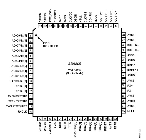 Specifications
| Parameter |
Rating |
ELECTRICAL AVDD, CLKVDD Voltage
DVDD, DRVDD Voltage
RX+, RX−, REFT, REFB
IOUTP+, IOUTP−
IOUTN+, IOUTN−, IOUTG+, IOUTG−
OSCIN, XTAL
REFIO, REFADJ
Digital Input and Output Voltage
Digital Output Current |
3.9 V maximum
3.9 V maximum
−0.3 V to AVDD + 0.3 V
−1.5 V to AVDD + 0.3 V
−0.3 V to +7 V
−0.3 V to CLVDD + 0.3 V
−0.3 V to AVDD + 0.3 V
−0.3 V to DRVDD + 0.3 V
5 mA maximum |
ENVIRONMENTAL Operating Temperature Range (Ambient)
Maximum Junction Temperature
Lead Temperature (Soldering, 10 s)
Storage Temperature Range (Ambient) |
−40 to +85
125
150
−65 to +150 |
DescriptionThe AD9865 is a mixed-signal front end (MxFE) IC for transceiver applications requiring Tx and Rx path functionality with data rates up to 80 MSPS. Its flexible digital interface, power saving modes, and high Tx-to-Rx isolation make it well suited for half- and full-duplex applications. The digital inter-face is extremely flexible allowing simple interfaces to digital back ends that support half- or full-duplex data transfers, thus often allowing the AD9865 to replace discrete ADC and DAC solutions. Power saving modes include the ability to reduce power consumption of individual functional blocks, or to power down unused blocks in half-duplex applications. A serial port interface (SPI®) allows software programming of the various functional blocks. An on-chip PLL clock multiplier and synthesizer provide all the required internal clocks, as well as two external clocks from a single crystal or clock source.
The AD9865 Tx signal path consists of a bypassable 2*/4* low-pass interpolation filter, a 10-bit TxDAC, and a line driver. The transmit path signal bandwidth can be as high as 34 MHz at an input data rate of 80 MSPS. The TxDAC provides differential current outputs that can be steered directly to an external loador to an internal low distortion current amplifier. The current amplifier (IAMP) can be configured as a current- or voltage-mode line driver (with two external npn transistors) capable of delivering in excess of 23 dBm peak signal power. Tx power can be digitally controlled over a 19.5 dB range in 0.5 dB steps.
The AD9865 receive path consists of a programmable amplifier (RxPGA), a tunable low-pass filter (LPF), and a 10-bit ADC. The low noise RxPGA has a programmable gain range of -12 dB to +48 dB in 1 dB steps. Its input referred noise is less than 3 nV/rtHz for gain settings beyond 36 dB. The receive path LPF cutoff frequency can be set over a 15 MHz to 35 MHz range or simply bypassed. The 10-bit ADC achieves excellent dynamic performance over a 5 MSPS to 80 MSPS span. Both the RxPGA and the ADC offer scalable power consumption allowing power/performance optimization.
The AD9865 provides a highly integrated solution for many broadband modems. It is available in a space saving 64-pin chip scale package and is specified over the commercial (-40 to +85) temperature range.
The AD9865 is a mixed-signal front end (MxFE®) IC for transceiver applications requiring Tx and Rx path functionality with data rates up to 80 MSPS. Its flexible digital interface, power saving

 AD9865 Data Sheet