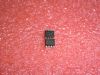
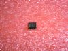
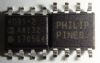
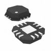
Pinout Description
The ADA4800 is voltage buffer integrated with an active load.The buffer is a low power, high speed, low noise, high slew rate,fast settling, fixed gain of 1 monolithic amplifier for chargecoupled device (CCD) applications. For CCD applications, the active load current source (IAL) can load the open source CCD sensor outputs and the buffer can drive the AFE load.
Features of the ADA4800 are:(1)integrated active load and gain of 1 buffer; (2)very low buffer power consumption as low as 20 mW on chip; (3)power save feature to reduce active load current by GPO control; (4)high buffer speed:400 MHz, -3 dB bandwidth,415 V/s slew rate; (5)fast settling time to 1%, 2 V step: 5 ns; (6)adjustable buffer bandwidth; (7)push-pull output stage; (8)adjustable active load current; (9)small package: 1.6 mm * 1.6 mm * 0.55 mm.The buffer of the ADA4800 employs a push-pull output stage architecture, providing drive current and maximum slew capability for both rising and falling signal transitions. At a 5 mA quiescent current setting, it provides 400 MHz, -3 dB bandwidth, which makes this buffer well suited for CCD sensors from machine vision to digital still camera applications.
The absolute maximum ratings of the ADA4800 can be summarized as:(1)operating temp:-40 to 85;(2)storage temperature range:-65 to +150;(3)junction temperature range:-65 to 150;(4)supply voltage:18V;(5)input voltage:VEE to VCC;(6)ISF pin:VEE to VCC.Stresses above those listed under Absolute Maximum Ratings may cause permanent damage to the device. This is a stress rating only; functional operation of the device at these or any other conditions above those indicated in the operational section of this specification is not implied.Exposure to absolute maximum rating conditions for extended periods may affect device reliability.The actual value is determined by the circuit transient and frequency requirements. In addition, 0.1 F MLCC decoupling capacitors should be located as close to the power supply pin as is physically possible, no more than 1/8 inch away. The ground returns should terminate immediately into the ground plane. Locating the bypass capacitor return close to the load return minimizes ground loops and improves performance.

 ADA4800 Data Sheet