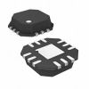
DescriptionThe ADA4930-1/ADA4930-2 are very low noise, low distortion, high speed differential amplifiers. They are an ideal choice for driving 1.8 V high performance ADCs with resolutions up to 14 bits from dc to 70 MHz. The low dc offset and excellent dynamic performance of the ADA4930-1/ADA4930-2 make them well suited for a wide variety of data acquisition and signal processing applications. The adjustable output common mode allows the ADA4930-1/ADA4930-2 to match the input of the ADC. The internal common-mode feedback loop provides exceptional output balance, suppression of even-order harmonic distortion products, and dc level translation. With the ADA4930-1/ADA4930-2, differential gain configurations are easily realized with a simple external feedback network of four resistors determining the closed-loop gain of the amplifier. The ADA4930-1/ADA4930-2 are fabricated using Analog Devices, Inc., proprietary silicon-germanium (SiGe), complementary bipolar process, enabling them to achieve very low levels of distortion with an input voltage noise of only 1.2 nV/Hz. The ADA4930-1 is available in a Pb-free, 3 mm * 3 mm 16-lead LFCSP, and the ADA4930-2 is available in a Pb-free, 4 mm * 4 mm 24-lead LFCSP. The pinout has been optimized to facilitate printed circuit board (PCB)layout and minimize distortion. The ADA4930-1 is specified to operate over the -40°C to +105°C temperature range, and the ADA4930-2 is specified to operate over the -40°C to +105°C temperature range for 3.3 V or 5 V supply voltages.
The features of ADA4930-1 can be summarized as (1)low input voltage noise: 1.2 nV/Hz; (2)low common-mode output: 0.9 V on single supply; (3)extremely low harmonic distortion -104 dBc HD2 at 10 MHz/ -79 dBc HD2 at 70 MHz/ -73 dBc HD2 at 100 MHz/ -101 dBc HD3 at 10 MHz/ -82 dBc HD3 at 70 MHz/ -75 dBc HD3 at 100 MHz; (4)high speed -3 dB bandwidth of 1.35 GHz, G = 1/ slew rate: 3400 V/s, 25% to 75%/ 0.1 dB gain flatness to 380 MHz/ fast overdrive recovery of 1.5 ns; (5)0.5 mV typical offset voltage; (6)externally adjustable gain; (7)differential-to-differential or single-ended-to-differential operation; (8)adjustable output common-mode voltage; (9)single-supply operation: 3.3 V or 5 V.
The absolute maximum ratings of ADA4930-1 are (1)supply voltage: 5.5 V; (2)power dissipation see: figure 4; (3)storage temperature range: -65°C to +125°C; (4)operating temperature range: -40°C to +105°C; (5)lead temperature (Soldering, 10 sec): 300°C; (6)junction temperature: 150°C.

 ADA4930-1 Data Sheet


