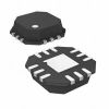
Features: High performance at low power High speed −3 dB bandwidth of 560 MHz, G = 1 0.1 dB gain flatness to 300 MHz Slew rate: 2800 V/s, 25% to 75% Fast 0.1% settling time of 9 ns Low power: 9.6 mA per amplifier Low harmonic distortion 100 dB SFDR @ 10 MHz 90 dB SFDR @ 20 MHz Low input...
ADA4932-1: Features: High performance at low power High speed −3 dB bandwidth of 560 MHz, G = 1 0.1 dB gain flatness to 300 MHz Slew rate: 2800 V/s, 25% to 75% Fast 0.1% settling time of 9 ns Low powe...
SeekIC Buyer Protection PLUS - newly updated for 2013!
268 Transactions
All payment methods are secure and covered by SeekIC Buyer Protection PLUS.

| Parameter | Rating |
| Supply Voltage Power Dissipation Input Current, +IN, −IN, PD Storage Temperature Range Operating Temperature Range ADA4932-1 ADA4932-2 Lead Temperature (Soldering, 10 sec) Junction Temperature |
11 V See Figure 4 ±5 mA −65 to +125 −40 to +105 −40 to +105 300 150 |
The ADA4932-x is the next generation AD8132 with higher performance, and lower noise and power consumption. It is an ideal choice for driving high performance ADCs as a single-ended-to-differential or differential-to-differential amplifier. The output common-mode voltage is user adjustable by means of an internal common-mode feedback loop, allowing the ADA4932-x output to match the input of the ADC. The internal feedback loop also provides exceptional output balance as well as suppression of even-order harmonic distortion products.
With the ADA4932-x, differential gain configurations are easily realized with a simple external four-resistor feedback network that determines the closed-loop gain of the amplifier.
The ADA4932-x is fabricated using the Analog Devices, Inc., proprietary silicon-germanium (SiGe) complementary bipolar process, enabling it to achieve low levels of distortion and noise at low power consumption. The low offset and excellent dynamic performance of the ADA4932-x make it well suited for a wide variety of data acquisition and signal processing applications.
The ADA4932-x is available in a Pb-free, 3 mm * 3 mm 16-lead LFCSP (ADA4932-1, single) or a Pb-free, 4 mm * 4 mm 24-lead LFCSP (ADA4932-2, dual). The pinout has been optimized to facilitate PCB layout and minimize distortion. The ADA4932-1 and the ADA4932-2 are specified to operate over the −40 to +105 temperature range; both operate on supplies between +3 V and ±5 V.